Datasheet4U Logo Datasheet4U.com

HCD71 - (HCD71 / HCD170) 12V OCXO Sine Output

Download the HCD71 datasheet PDF. This datasheet also covers the HCD170 variant, as both devices belong to the same (hcd71 / hcd170) 12v ocxo sine output family and are provided as variant models within a single manufacturer datasheet.
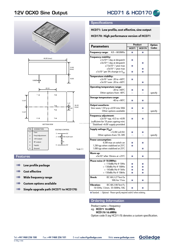
Features

  • ࡯ ࡯ ࡯ ࡯ ࡯ ࡯ ࡯ ➠ ➠ ➠ ➠ ➠ Low profile package Cost effective Wide frequency range Custom options available Simple upgrade path (HCD71 to HCD170) Vibration: IEC 68-2-06 Test Fc 10-55Hz, 1.5mm. 55-500Hz, 10G ࡯ Standard. ˿ Optional - Please specify required code(s) when ordering Ordering Information Product name + frequency eg: HCD71 10.0MHz HCD170 10.0MHz Option code X (eg HCD71/X) denotes a custom specification. Tel: +44 1460 256 100 01 May 1998 Fax: +44 1460 256 101 E-mail: sales@golledge.

📥 Download Datasheet

Note: The manufacturer provides a single datasheet file (HCD170_GolledgeElectronics.pdf) that lists specifications for multiple related part numbers.

Datasheet Details

Part number HCD71
Manufacturer Golledge Electronics
File Size 92.93 KB
Description (HCD71 / HCD170) 12V OCXO Sine Output
Datasheet download datasheet HCD71 Datasheet

Full PDF Text Transcription (Reference)

The following content is an automatically extracted verbatim text from the original manufacturer datasheet and is provided for reference purposes only.

View original datasheet text
12V OCXO Sine Output HCD71 & HCD170 Specifications HCD71: Low profile, cost effective, sine output HCD170: High performance version of HCD71 Product HCD71 HCD170 Parameters Frequency range: 46.00 (max) Option Codes 4.0 ~ 60.0MHz ࡯ ࡯ ࡯ ࡯ ࡯ ࡯ 15.00 (max) Frequency stability: ±1x10⁻⁸ / day at despatch ±5x10⁻⁹ / day at despatch ±7.5x10⁻⁷ / year max ±5x10⁻⁷ / year max ±1x10⁻⁷ per 5% change in VDD Temperature stability: ±2x10⁻⁷ over -20 to +60°C ±5x10⁻⁸ over -20 to +60°C Operating temperature range: -20 to +60°C Other options from -40°C Storage temperature range: -40 to +90°C ࡯ ࡯ ࡯ 0.80Ø 10.00 ࡯ ࡯ ˿ ࡯ ࡯ ˿ ࡯ 20.32 1 13.97 3 4 13.97 6 BOTTOM VIEW PIN 1 2 3 4 5 6 CONNECTION Case Freq Adjustment +6V output RF output Supply Ground 6 VOLTAGE CONTROL 3 2 6V 10k multi-turn 1k 0V 5 1.27 3.
Published: |