Datasheet4U Logo Datasheet4U.com

HM4612 - N & P-Channel Enhancement Mode Power MOSFET

Datasheet Summary

Features

  • Advanced trench process technology High Density Cell Design For Ultra Low On-Resistance Improved Shoot-Through FOM Package Dimensions 4612 REF. A B C D E F Millimeter Min. Max. 5.80 6.20 4.80 5.00 3.80 4.00 0° 8° 0.40 0.90 0.19 0.25 REF. M H L J K G Millimeter Min. Max. 0.10 0.25 0.35 0.49 1.35 1.75 0.375 REF. 45° 1.27 TYP. Maximum Ratings and Thermal Characteristics (TA = 25oC unless otherwise noted) 25 oC Parameter Drain-Source Voltage Symbol VDS Ra.

📥 Download Datasheet

Datasheet preview – HM4612

Datasheet Details

Part number HM4612
Manufacturer H&M Semiconductor
File Size 325.96 KB
Description N & P-Channel Enhancement Mode Power MOSFET
Datasheet download datasheet HM4612 Datasheet
Additional preview pages of the HM4612 datasheet.
Other Datasheets by H&M Semiconductor

Full PDF Text Transcription

Click to expand full text
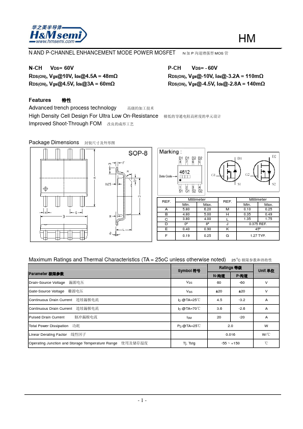
N AND P-CHANNEL ENHANCEMENT MODE POWER MOSFET N P MOS HM N-CH VDS= 60V RDS(ON), Vgs@10V, Ids@4.5A = 48mΩ RDS(ON), Vgs@4.5V, Ids@3A = 60mΩ P-CH VDS= - 60V RDS(ON), Vgs@-10V, Ids@-3.2A = 110mΩ RDS(ON), Vgs@-4.5V, Ids@-2.8A = 140mΩ Features Advanced trench process technology High Density Cell Design For Ultra Low On-Resistance Improved Shoot-Through FOM Package Dimensions 4612 REF. A B C D E F Millimeter Min. Max. 5.80 6.20 4.80 5.00 3.80 4.00 0° 8° 0.40 0.90 0.19 0.25 REF. M H L J K G Millimeter Min. Max. 0.10 0.25 0.35 0.49 1.35 1.75 0.375 REF. 45° 1.27 TYP.
Published: |