2SK2595
Features
- High power output, High gain, High efficiency PG = 7.8d B, Pout = 37.3d Bm, ηD = 50 %min. (f = 836.5MHz)
- pact package capable of surface mounting
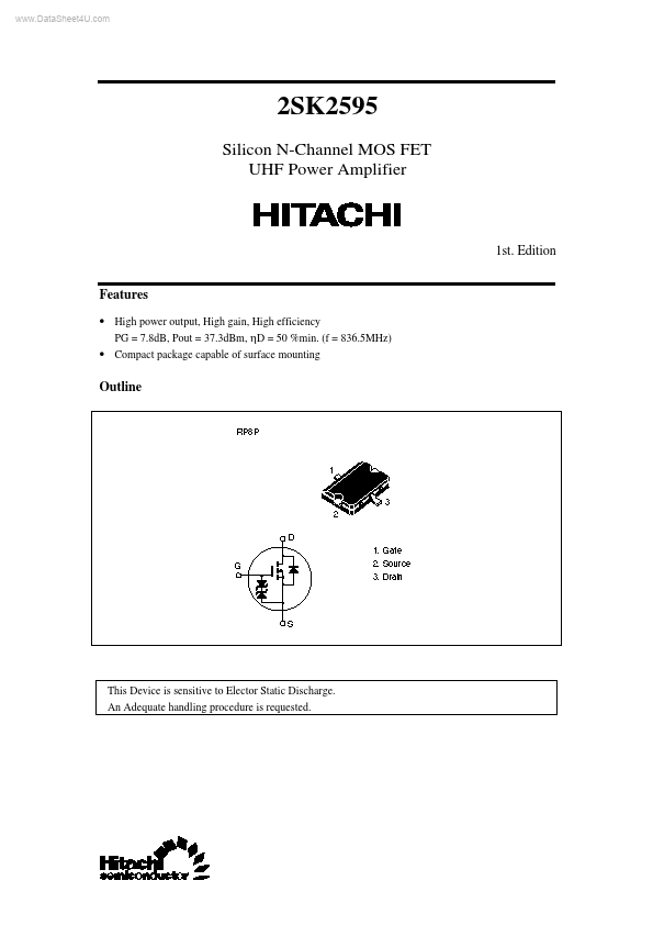
Outline
This Device is sensitive to Elector Static Discharge. An Adequate handling procedure is requested.
Absolute Maximum Ratings (Ta = 25°C)
Item Drain to source voltage Gate to source voltage Drain current Drain peak current Channel dissipation Channel temperature Storage temperature Notes: 1. PW ≤ 10 µs, duty cycle ≤ 1 % 2. Value at Tc = 25°C Symbol VDSS VGSS ID I D(pulse)- Pch- Tch Tstg
2 1
Ratings 17 ±10 1.1 5 20 150
- 45 to +150
Unit V V A A W °C °C
Electrical Characteristics (Ta = 25°C)
Item Zero gate voltage drain current Gate to source leak current Gate to source cutoff voltage Input capacitance Output capacitance Output Power Symbol I DSS I GSS VGS(off) Ciss Coss Pout Min.
- - 0.6
- - 37.3 Typ
- -
- 68 27 38.45 Max. 10 ±5.0 1.3
- -
- Unit µA µA V p F p F d Bm Test Conditions VDS = 12 V, VGS = 0 VGS = ±10V,...