Datasheet4U Logo Datasheet4U.com

HY5DU281622T-L - 4 Banks x 2M x 16Bit Double Data Rate SDRAM

Download the HY5DU281622T-L datasheet PDF. This datasheet also covers the HY5DU281622 variant, as both devices belong to the same 4 banks x 2m x 16bit double data rate sdram family and are provided as variant models within a single manufacturer datasheet.

Description

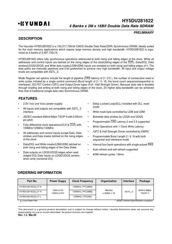
The Hyundai HY5DU281622 is a 134,217,728-bit CMOS Double Data Rate(DDR) Synchronous DRAM, ideally suited for the main memory applications which require large memory density and high bandwidth.

HY5DU281622 is organized as 4 banks of 2,097,152x16.

Features

  • 2.5V V DD and VDDQ power suppliy All inputs and outputs are compatible with SSTL_2 interface JEDEC standard 400mil 66pin TSOP-II with 0.65mm pin pitch Fully differential clock operations(CLK & CLK) with 100MHz/125MHz/133MHz All addresses and control inputs except Data, Data strobes and Data masks latched on the rising edges of the clock Data(DQ) and Write masks(LDM/UDM) latched on both rising and falling edges of the Data Stobe Data outputs on LD.

📥 Download Datasheet

Note: The manufacturer provides a single datasheet file (HY5DU281622-Hyundai.pdf) that lists specifications for multiple related part numbers.

Datasheet Details

Part number HY5DU281622T-L
Manufacturer Hyundai
File Size 83.14 KB
Description 4 Banks x 2M x 16Bit Double Data Rate SDRAM
Datasheet download datasheet HY5DU281622T-L Datasheet

Full PDF Text Transcription

Click to expand full text
HY5DU281622 4 Banks x 2M x 16Bit Double Data Rate SDRAM PRELIMINARY DESCRIPTION The Hyundai HY5DU281622 is a 134,217,728-bit CMOS Double Data Rate(DDR) Synchronous DRAM, ideally suited for the main memory applications which require large memory density and high bandwidth. HY5DU281622 is organized as 4 banks of 2,097,152x16. HY5DU281622 offers fully synchronous operations referenced to both rising and falling edges of the clock. While all addresses and control inputs are latched on the rising edges of the clock(falling edges of the CLK), Data(DQ), Data strobes(LDQS/UDQS) and Write data masks(LDM/UDM) inputs are sampled on both rising and falling edges of it. The data paths are internally pipelined and 2-bit prefetched to achieve very high bandwidth.
Published: |