Datasheet4U Logo Datasheet4U.com

ICSSSTUB32872A - 28-Bit Registered Buffer

Description

This 28-bit 1:1 registered buffer with parity is designed for 1.7V to 1.9V VDD operation.

All clock and data inputs are compatible with the JEDEC standard for SSTL_18.

The control inputs are LVCMOS.

Features

  • 28-bit 1:1 registered buffer with parity check functionality.
  • Supports SSTL_18 JEDEC specification on data inputs and outputs.
  • Supports LVCMOS switching levels on RESET input.
  • 50% more dynamic driver strength than standard SSTU32864.
  • Low voltage operation VDD = 1.7V to 1.9V.
  • Available in 96 BGA package
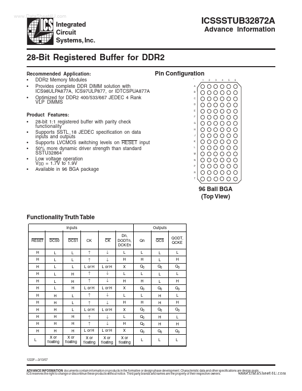
 Pin Configuration 1 A B C D E F G H J K L M N P R T 2 3 4 5 6 96 Ball BGA (Top View) Functionality Truth Table In puts RESET H H H H H H.

📥 Download Datasheet

Datasheet Details

Part number ICSSSTUB32872A
Manufacturer ICS
File Size 238.50 KB
Description 28-Bit Registered Buffer
Datasheet download datasheet ICSSSTUB32872A Datasheet

Full PDF Text Transcription

Click to expand full text
www.DataSheet4U.com Integrated Circuit Systems, Inc. ICSSSTUB32872A Advance Information 28-Bit Registered Buffer for DDR2 Recommended Application: • DDR2 Memory Modules • Provides complete DDR DIMM solution with ICS98ULPA877A, ICS97ULP877, or IDTCSPUA877A • Optimized for DDR2 400/533/667 JEDEC 4 Rank VLP DIMMS Product Features: • 28-bit 1:1 registered buffer with parity check functionality • Supports SSTL_18 JEDEC specification on data inputs and outputs • Supports LVCMOS switching levels on RESET input • 50% more dynamic driver strength than standard SSTU32864 • Low voltage operation VDD = 1.7V to 1.
Published: |