ICSSSTUB32864A
ICSSSTUB32864A is 25-Bit Configurable Registered Buffer manufactured by ICS.
..
Integrated Circuit Systems, Inc.
Advance Information
25-Bit Configurable Registered Buffer for DDR2
Remended Application:
- DDR2 Memory Modules
- Provides plete DDR DIMM solution with ICS97U877
- Ideal for DDR2 400, 533, 667 and 800 Product Features
:
- 25-bit 1:1 or 14-bit 1:2 configurable registered buffer
- Supports SSTL_18 JEDEC specification on data inputs and outputs
- Supports LVCMOS switching levels on C0, C1 and RESET# inputs
- Low voltage operation VDD = 1.7V to 1.9V
- Available in 96 BGA package
- Drop-in replacement for ICSSSTUB32866
- Green packages available
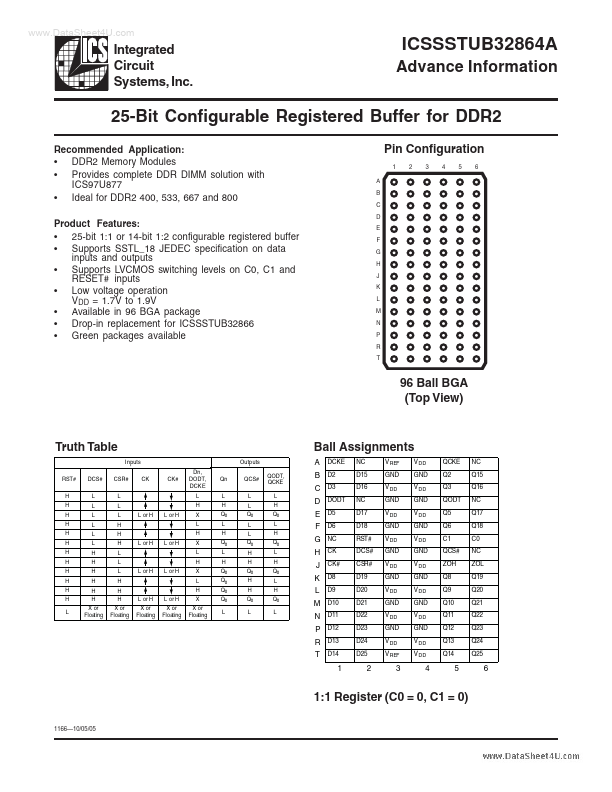
Pin Configuration
1 A B C D E F G H J K L M N P R T 2 3 4 5 6
96 Ball BGA (Top View)
Truth Table
I nputs RST# H H H H H H H H H H H H L DCS# L L L L L L H H H H H H X or Floating CSR# L L L H H H L L L H H H X or Floating L or H X or Floating L or H X or Floating L or H L or H L or H L or H L or H L or H CK CK# Dn, DODT, DCK E L H X L H X L H X L H X X or Floating Qn L H Q0 L H Q0 L H Q0 Q0 Q0 Q0 L Outputs QCS# L L Q0 L L Q0 H H Q0 H H Q0 L QODT, QCKE L H Q0 L H Q0 L H Q0 L H Q0 L
Ball Assignments
A DCKE B D2 C D3 D DODT E
D5 NC D15 D16 NC D17 D18 RST# DCS# CSR# D19 D20 D21 D22 D23 D24 D25 V REF GND V DD GND V DD GND V DD GND V DD GND V DD GND V DD GND V DD V REF V DD GND V DD GND V DD GND V DD GND V DD GND V DD GND V DD GND V DD V DD QCKE Q2 Q3 QODT Q5 Q6 C1 QCS# ZOH Q8 Q9 Q10 Q11 Q12 Q13 Q14 NC Q15 Q16 NC Q17 Q18 C0 NC ZOL Q19 Q20 Q21 Q22 Q23 Q24 Q25
F D6 G NC H CK J K D8
CK#
L D9 M D10 N D11 P D12 R
D13
T D14 1
1:1 Register (C0 = 0, C1 =...