ICSSSTUB32872A
ICSSSTUB32872A is 28-Bit Registered Buffer manufactured by ICS.
..
Integrated Circuit Systems, Inc.
Advance Information
28-Bit Registered Buffer for DDR2
Remended Application:
- DDR2 Memory Modules
- Provides plete DDR DIMM solution with ICS98ULPA877A, ICS97ULP877, or IDTCSPUA877A
- Optimized for DDR2 400/533/667 JEDEC 4 Rank VLP DIMMS Product Features
:
- 28-bit 1:1 registered buffer with parity check functionality
- Supports SSTL_18 JEDEC specification on data inputs and outputs
- Supports LVCMOS switching levels on RESET input
- 50% more dynamic driver strength than standard SSTU32864
- Low voltage operation VDD = 1.7V to 1.9V
- Available in 96 BGA package
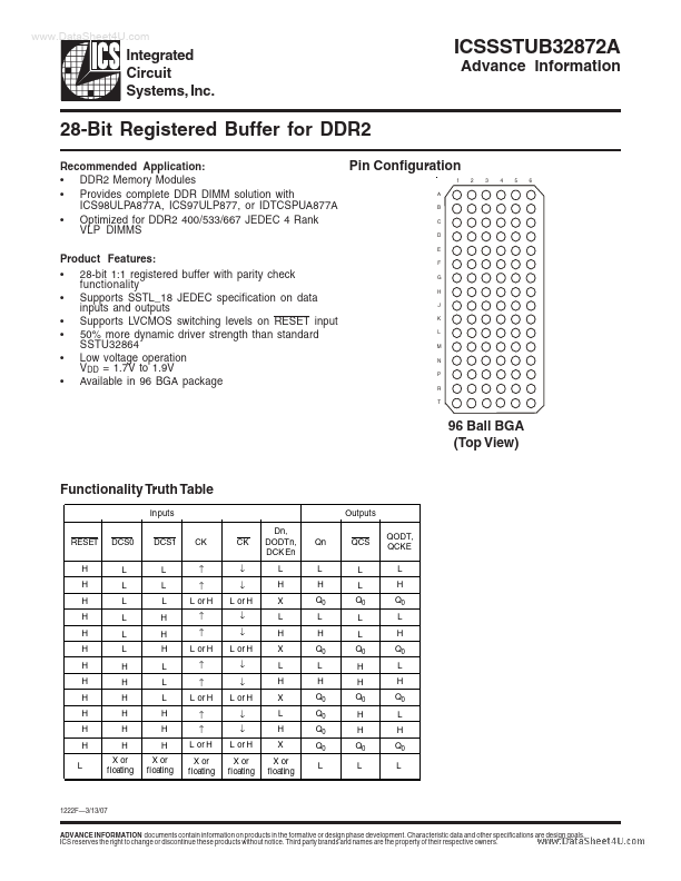
Pin Configuration
1 A B C D E F G H J K L M N P R T 2 3 4 5 6
96 Ball BGA (Top View)
Functionality Truth Table
In puts RESET H H H H H H H H H H H H L DCS0 L L L L L L H H H H H H X or floating DCS1 L L L H H H L L L H H H X or floating CK ↑ ↑ L or H ↑ ↑ L or H ↑ ↑ L or H ↑ ↑ L or H X or floating CK ↓ ↓ L or H ↓ ↓ L or H ↓ ↓ L or H ↓ ↓ L or H X or floating Dn, DODTn, DCK En L H X L H X L H X L H X X or floating Qn L H Q0 L H Q0 L H Q0 Q0 Q0 Q0 L Outputs QCS L L Q0 L L Q0 H H Q0 H H Q0 L QODT, QCKE L H Q0 L H Q0 L H Q0 L H Q0 L
1222F- 3/13/07
ADVANCE INFORMATION documents contain information on products in the formative or design phase development. Characteristic data and other specifications are design goals. ICS reserves the right to change or discontinue these products without notice. Third party brands and names are the property of their respective owners.
Advance Information
Ball Assignments 28 bit 1:1 Register
A DCKE0 D0 B DCKE1 D1 C D2 E
D3 DODT1 V REF GND V DD V DD GND V DD GND V DD GND V DD GND V DD GND V DD GND V DD GND V DD V DD QCKE0 Q0 Q2 QODT0 Q3 Q5 NC QCS0 NC Q7 Q9 Q11 Q13 Q15 Q17 Q19 QCKE1 Q1 Q21 QODT1 Q4 Q6 NC QCS1 NC Q8 Q10 Q12 Q14 Q16 Q18 Q20
D DODT0 PTYERR GND
D4 D6 V DD GND
F D5 H CK J CK K L
D7...