ICS ICSSSTUB32871A
The ICSSSTUB32871A operates from a differential clock (CK and CK). The device supports low-power standby operation. When the reset input (RESET) is low, the differential input receivers are disabled, and undriven (floating) data, clock and reference voltage (VREF) inputs are allowed.| Part No. | ICSSSTUB32871A |
|---|---|
| Datasheet | ICSSSTUB32871A Download |
| Manufacturer |  ICS |
| Description | 27-Bit Registered Buffer |
| Buy | Stock & Price |
FEATURES
:● 27-bit 1:1 registered buffer with parity check functionality
● Supports SSTL_18 JEDEC specification on data inputs and outputs
● Supports LVCMOS switching levels on RESET input
● 50% more dynamic driver strength than standard SSTU32864
● Low voltage operation VDD = 1.7V to 1.9V
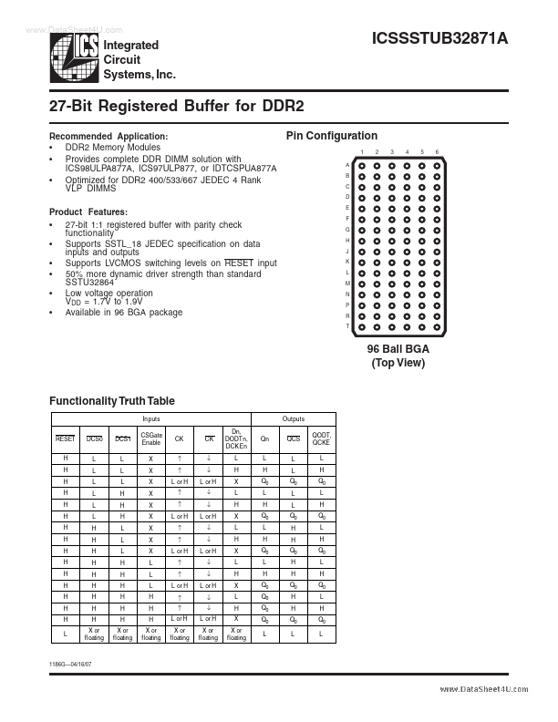
● Available in 96 BGA package Pin Configuration 1 A B C D E F G H J K L M N P R T 2 3 4 5 6 96 Ball BGA (Top View) Functionality Truth Table In puts RESET H H H H H H H H H H H H H H H L DCS0 L L L L L L H H H H H H H H H X or floating DCS1 L L L H H H L L L H H H H H H X or floating CSGate Enable X X X X X X X X X L L L H H H X or floating CK ↑ ↑ L or H ↑ ↑ L or H ↑ ↑ L or H ↑ ↑ L or H ↑ ↑ L or H X or floating CK ↓ ↓ L or H ↓ ↓ L or H ↓ ↓ L or H ↓ ↓ L or H ↓ ↓ L or H X or floating Dn, DODTn, DCK En L H X L H X L H X L H X L H X X or floating Qn L H Q0 L H Q0 L H Q0 L H Q0 Q0 Q0 Q0 L Outputs QCS L L Q0 L L Q0 H H Q0 H H Q0 H H Q0 L QODT, QCKE L H Q0 L H Q0 L H Q0 L H Q0 L H Q0 L 1186G—04/16/07 ICSSST...

