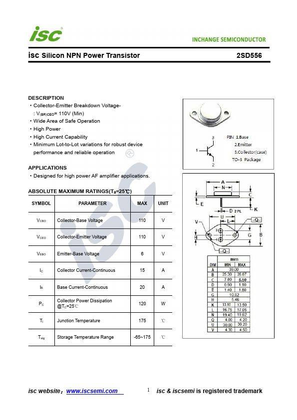
Collector-Emitter Breakdown Voltage-
: V(BR)CEO= 110V (Min)
Wide Area of Safe Operation
High Power
High Current Capability
Minimum Lot-to-Lot variations for robust device
performance and reliable operation
APPLICATIONS
Designed for high power AF amplifier applications.
The following content is an automatically extracted verbatim text
from the original manufacturer datasheet and is provided for reference purposes only.
View original datasheet text
isc Silicon NPN Power Transistor
INCHANGE Semiconductor
2SD556
DESCRIPTION ·Collector-Emitter Breakdown Voltage-
: V(BR)CEO= 110V (Min) ·Wide Area of Safe Operation ·High Power ·High Current Capability ·Minimum Lot-to-Lot variations for robust device
performance and reliable operation
APPLICATIONS ·Designed for high power AF amplifier applications.
ABSOLUTE MAXIMUM RATINGS(Ta=25℃)
SYMBOL
PARAMETER
MAX
UNIT
VCBO
Collector-Base Voltage
110
V
VCEO
Collector-Emitter Voltage
110
V
VEBO
Emitter-Base Voltage
6
V
IC
Collector Current-Continuous
15
A
IB
Base Current-Continuous
PC
Collector Power Dissipation @TC=25℃
Tj
Junction Temperature
20
A
120
W
175
℃
Tstg
Storage Temperature Range
-65~175 ℃
isc website:www.iscsemi.