BD650F Overview
Key Specifications
Max Operating Temp: 150 °C
Description
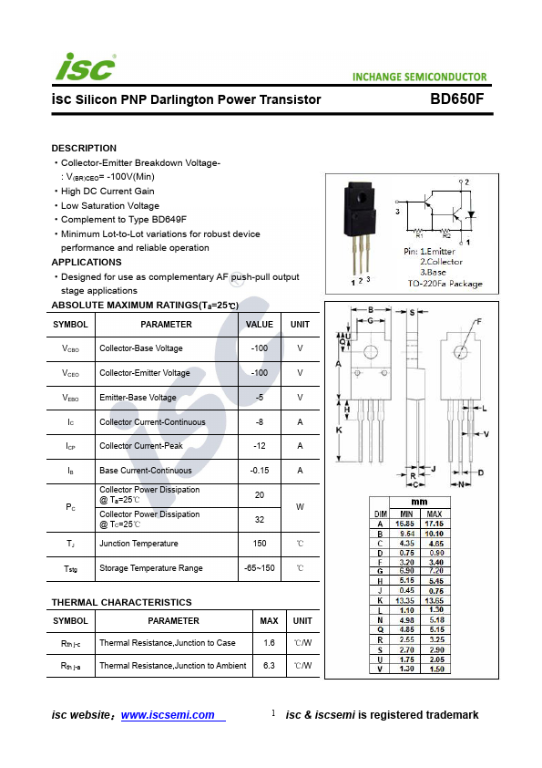
Collector-Emitter Breakdown Voltage- : V(BR)CEO= -100V(Min) - High DC Current Gain - Low Saturation Voltage - Complement to Type BD649F - Minimum Lot-to-Lot variations for robust device performance and reliable operation APPLICATIONS - Designed for use as complementary AF push-pull output stage applications SYMBOL PARAMETER VALUE UNIT VCBO Collector-Base Voltage -100 V VCEO Collector-Emitter Voltage -100 V VEBO Emitter-Base Voltage -5 V IC Collector Current-Continuous -8 A ICP Collector Current-Peak -12 A IB Base Current-Continuous Collector Power Dissipation @ Ta=25℃ PC Collector Power Dissipation @ TC=25℃ TJ Junction Temperature -0.15 A 20 W 32 150 ℃ Tstg Storage Temperature Range -65~150 ℃ SYMBOL PARAMETER MAX UNIT Rth j-c 1.6 ℃/W Rth j-a isc website: 1 isc & iscsemi is registered trademark isc Silicon PNP Darlington Power Transistor INCHANGE Semiconductor BD650F TC=25℃ unless otherwise specified SYMBOL PARAMETER CONDITIONS VCEO(SUS) Collector-Emitter Breakdown Voltage IC= -30mA; IB= 0 VCE(sat)-1 Collector-Emitter Saturation Voltage IC= -3A; IB= -12mA VCE(sat)-2 Collector-Emitter Saturation Voltage IC= -5A; IB= -50mA VBE(sat) Base-Emitter Saturation Voltage IC= -5A; IB= -50mA VBE(on) Base-Emitter On Voltage IC= -3A ; VCE= -3V ICBO Collector Cutoff Current VCB= -100V; IE= 0 VCB= -60V; IE= 0; TC= 150℃ ICEO Collector Cutoff Current VCE= -50V; IB= 0 IEBO Emitter Cutoff Current VEB= -5V; IC= 0 hFE-1 DC Current Gain IC= -0.5A ; VCE= -3V hFE-2 DC Current Gain IC= -3A ; VCE= -3V hFE-3 DC Current Gain IC= -8A ; VCE= -3V MIN TYP. MAX UNIT -100 V -2.0 V -2.5 V -3.0 V -2.5 V -0.1 mA -1.0 -0.5 mA -5.