BFG193 Overview
Description
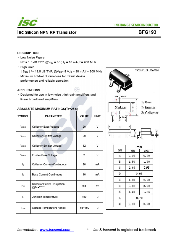
Low Noise Figure NF = 1.3 dB TYP. @VCE = 8 V, IC = 10 mA, f = 900 MHz - High Gain ︱S21e︱2 = 13.5 dB TYP.
| Part | BFG193 |
|---|---|
| Description | NPN Transistor |
| Category | Transistor |
| Manufacturer | Inchange Semiconductor |
| Size | 205.21 KB |
Low Noise Figure NF = 1.3 dB TYP. @VCE = 8 V, IC = 10 mA, f = 900 MHz - High Gain ︱S21e︱2 = 13.5 dB TYP.
| Part Number | Manufacturer | Description |
|---|---|---|
| BFG193 | Infineon | NPN Silicon RF Transistor |
| BFG193 | Siemens Semiconductor Group | NPN Silicon RF Transistor |
| BFG198 | NXP Semiconductors | NPN 8GHz wideband transistor |
| BFG196 | Siemens Semiconductor Group | NPN Silicon RF Transistor |
| BFG196 | Infineon | NPN Silicon RF Transistor |