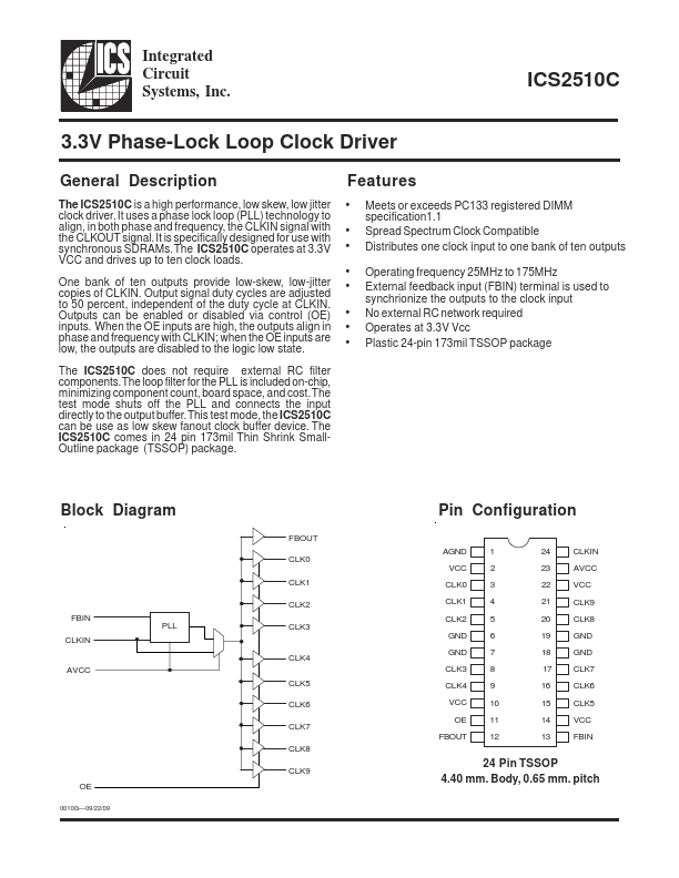
Datasheet4U Logo Datasheet4U.com

ICS2510C - 3.3V Phase-Lock Loop Clock Driver

Description

The ICS2510C is a high performance, low skew, low jitter clock driver.

It uses a phase lock loop (PLL) technology to align, in both phase and frequency, the CLKIN signal with the CLKOUT signal.

It is specifically designed for use with synchronous SDRAMs.

Features

  • Meets or exceeds PC133 registered DIMM specification1.1 Spread Spectrum Clock Compatible Distributes one clock input to one bank of ten outputs Operating frequency 25MHz to 175MHz External feedback input (FBIN) terminal is used to synchrionize the outputs to the clock input No external RC network required Operates at 3.3V Vcc Plastic 24-pin 173mil TSSOP package Block Diagram FBOUT CLK0 CLK1 CLK2 FBIN CLKIN PLL CLK3.

📥 Download Datasheet

Datasheet preview – ICS2510C

Datasheet Details

Part number ICS2510C
Manufacturer Integrated Circuit Systems
File Size 77.30 KB
Description 3.3V Phase-Lock Loop Clock Driver
Datasheet download datasheet ICS2510C Datasheet
Additional preview pages of the ICS2510C datasheet.
Other Datasheets by Integrated Circuit Systems

Full PDF Text Transcription

Click to expand full text
Integrated Circuit Systems, Inc. ICS2510C 3.3V Phase-Lock Loop Clock Driver General Description The ICS2510C is a high performance, low skew, low jitter clock driver. It uses a phase lock loop (PLL) technology to align, in both phase and frequency, the CLKIN signal with the CLKOUT signal. It is specifically designed for use with synchronous SDRAMs. The ICS2510C operates at 3.3V VCC and drives up to ten clock loads. One bank of ten outputs provide low-skew, low-jitter copies of CLKIN. Output signal duty cycles are adjusted to 50 percent, independent of the duty cycle at CLKIN. Outputs can be enabled or disabled via control (OE) inputs.
Published: |