Datasheet4U Logo Datasheet4U.com

IDT8P34S1208I - 1:8 LVDS Output 1.8V Fanout Buffer

General Description

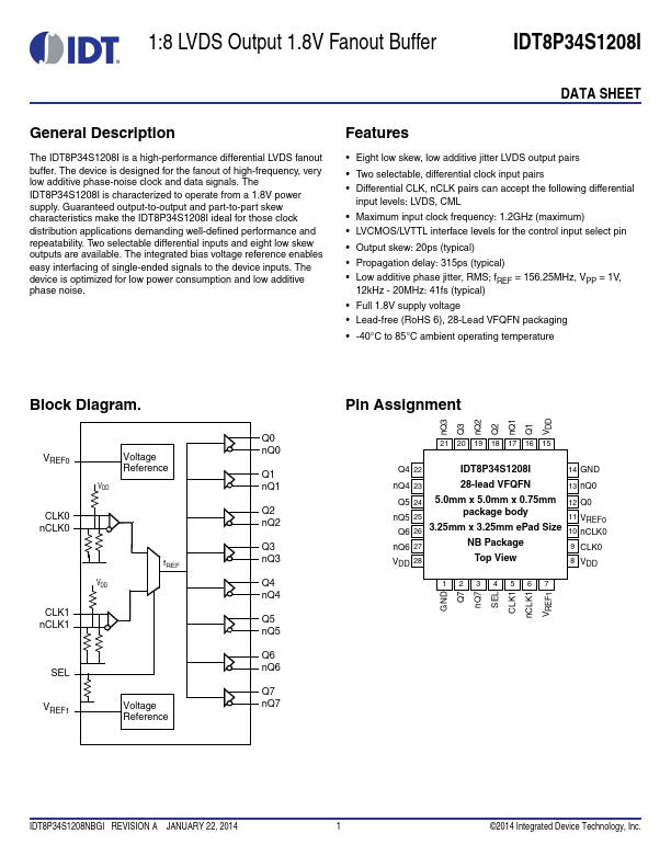
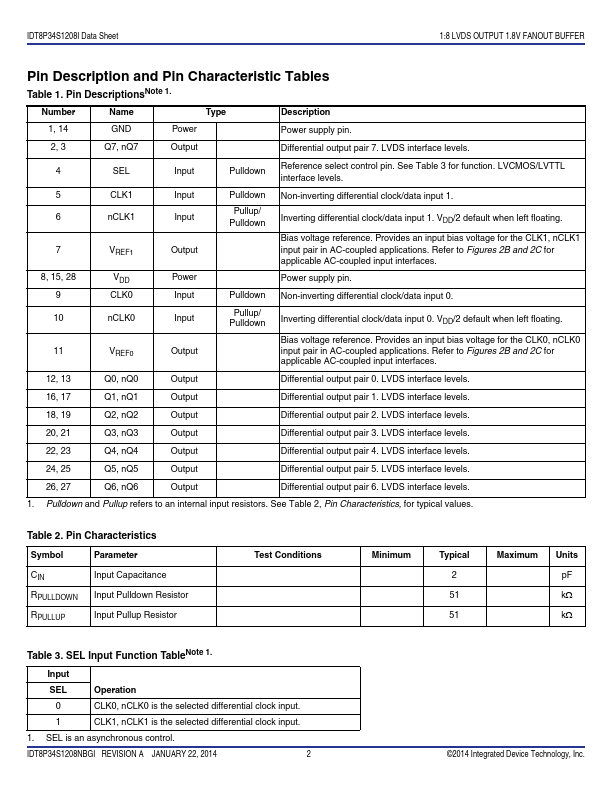
The IDT8P34S1208I is a high-performance differential LVDS fanout buffer.

The device is designed for the fanout of high-frequency, very low additive phase-noise clock and data signals.

The IDT8P34S1208I is characterized to operate from a 1.8V power supply.

Key Features

  • Eight low skew, low additive jitter LVDS output pairs Two selectable, differential clock input pairs Differential CLK, nCLK pairs can accept the following differential input levels: LVDS, CML Maximum input clock frequency: 1.2GHz (maximum) LVCMOS/LVTTL interface levels for the control input select pin Output skew: 20ps (typical) Propagation delay: 315ps (typical) Low additive phase jitte.

📥 Download Datasheet

Datasheet Details

Part number IDT8P34S1208I
Manufacturer Integrated Device
File Size 252.16 KB
Description 1:8 LVDS Output 1.8V Fanout Buffer
Datasheet download datasheet IDT8P34S1208I Datasheet

Full PDF Text Transcription for IDT8P34S1208I (Reference)

Note: Below is a high-fidelity text extraction (approx. 800 characters) for IDT8P34S1208I. For precise diagrams, and layout, please refer to the original PDF.

1:8 LVDS Output 1.8V Fanout Buffer IDT8P34S1208I DATA SHEET General Description The IDT8P34S1208I is a high-performance differential LVDS fanout buffer. The device is des...

View more extracted text
a high-performance differential LVDS fanout buffer. The device is designed for the fanout of high-frequency, very low additive phase-noise clock and data signals. The IDT8P34S1208I is characterized to operate from a 1.8V power supply. Guaranteed output-to-output and part-to-part skew characteristics make the IDT8P34S1208I ideal for those clock distribution applications demanding well-defined performance and repeatability. Two selectable differential inputs and eight low skew outputs are available. The integrated bias voltage reference enables easy interfacing of single-ended signals to the device inputs. The device is opt