Datasheet4U Logo Datasheet4U.com

IDT71V546 - 128K x 36/ 3.3V Synchronous SRAM with ZBT Feature/ Burst Counter and Pipelined Outputs

This page provides the datasheet information for the IDT71V546, a member of the IDT-71V 128K x 36/ 3.3V Synchronous SRAM with ZBT Feature/ Burst Counter and Pipelined Outputs family.

Description

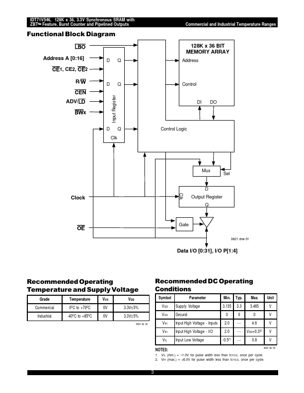
The IDT71V546 is a 3.3V high-speed 4,718,592-bit (4.5 Megabit) synchronous SRAM organized as 128K x 36 bits.

It is designed to eliminate dead bus cycles when turning the bus around between reads and writes, or writes and reads.

Thus it has been given the name ZBTTM, or Zero Bus Turn-around.

Features

  • 128K x 36 memory configuration, pipelined outputs Supports high performance system speed - 133 MHz (4.2 ns Clock-to-Data Access) ZBTTM Feature - No dead cycles between write and read cycles Internally synchronized registered outputs eliminate the need to control OE Single R/W (READ/WRITE) control pin Positive clock-edge triggered address, data, and control signal registers for fully pipelined.

📥 Download Datasheet

Datasheet preview – IDT71V546

Datasheet Details

Part number IDT71V546
Manufacturer Integrated Device Technology
File Size 178.20 KB
Description 128K x 36/ 3.3V Synchronous SRAM with ZBT Feature/ Burst Counter and Pipelined Outputs
Datasheet download datasheet IDT71V546 Datasheet
Additional preview pages of the IDT71V546 datasheet.
Other Datasheets by Integrated Device Technology

Full PDF Text Transcription

Click to expand full text
128K x 36, 3.3V Synchronous IDT71V546 SRAM with ZBT™ Feature, Burst Counter and Pipelined Outputs Features 128K x 36 memory configuration, pipelined outputs Supports high performance system speed - 133 MHz (4.2 ns Clock-to-Data Access) ZBTTM Feature - No dead cycles between write and read cycles Internally synchronized registered outputs eliminate the need to control OE Single R/W (READ/WRITE) control pin Positive clock-edge triggered address, data, and control signal registers for fully pipelined applications 4-word burst capability (interleaved or linear) Individual byte write (BW1 - BW4) control (May tie active) Three chip enables for simple depth expansion Single 3.
Published: |