Datasheet Summary
- 97083
DirectFET Power MOSFET
RoHS pliant l Lead-Free (Qualified up to 260°C Reflow) l Application Specific MOSFETs l Ideal for CPU Core DC-DC Converters l Low Conduction Losses and Switching Losses l Low Profile (<0.7mm) l Dual Sided Cooling patible l patible with existing Surface Mount Techniques l
IRF6633PbF IRF6633TRPbF
RDS(on) RDS(on)
Typical values (unless otherwise specified)
VDSS
20V max ±20V max 4.1mΩ @ 10V 7.0mΩ @ 4.5V
Qg tot
Qgd
4.0nC
Qgs2
1.2nC
Qrr
32nC
Qoss
8.8nC
Vgs(th)
1.8V
11nC
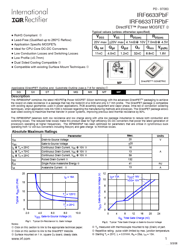
Applicable DirectFET Outline and Substrate Outline (see p.7,8 for details) SQ SX ST MQ MX MT MP
DirectFET ISOMETRIC
Description
The IRF6633PbF bines...