JMTP9435A
Description
JMT P-channel Enhancement Mode Power MOSFET
Features
- VDS= -30V, ID= -5.1A RDS(ON) <55mΩ @ VGS = -10V RDS(ON) <90mΩ @ VGS = -4.5V
- Advanced Trench Technology
- Excellent RDS(ON) and Low Gate Charge
- Lead free product is acquired
Application
- PWM Applications
- Load Switch
- Power Management
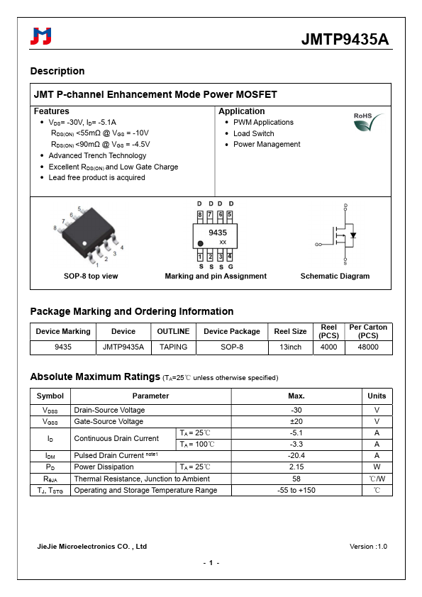
SOP-8 top view
Marking and pin Assignment
Schematic Diagram
Package Marking and Ordering Information
Device Marking 9435
Device JMTP9435A
OUTLINE TAPING
Device Package SOP-8
Reel Size 13inch
Reel (PCS)
Per Carton (PCS)
Absolute Maximum Ratings (TA=25℃ unless otherwise specified)
Symbol VDSS VGSS
IDM PD RθJA TJ, TSTG
Parameter
Drain-Source Voltage
Gate-Source Voltage
Continuous Drain Current Pulsed Drain Current note1
TA = 25℃ TA = 100℃
Power Dissipation
TA = 25℃
Thermal Resistance, Junction to Ambient
Operating and Storage Temperature Range
Max.
-30 ±20 -5.1 -3.3 -20.4 2.15 58 -55 to...