SI2301A
Key Features
- Halogen free available upon request by adding suffix "-HF"
- -20V,-2.8A, RDS(ON)=120mΩ@VGS=-4.5V RDS(ON)=150mΩ@VGS=-2.5V
- High dense cell design for extremely low RDS(ON)
- Rugged and reliable
- High Speed Switching
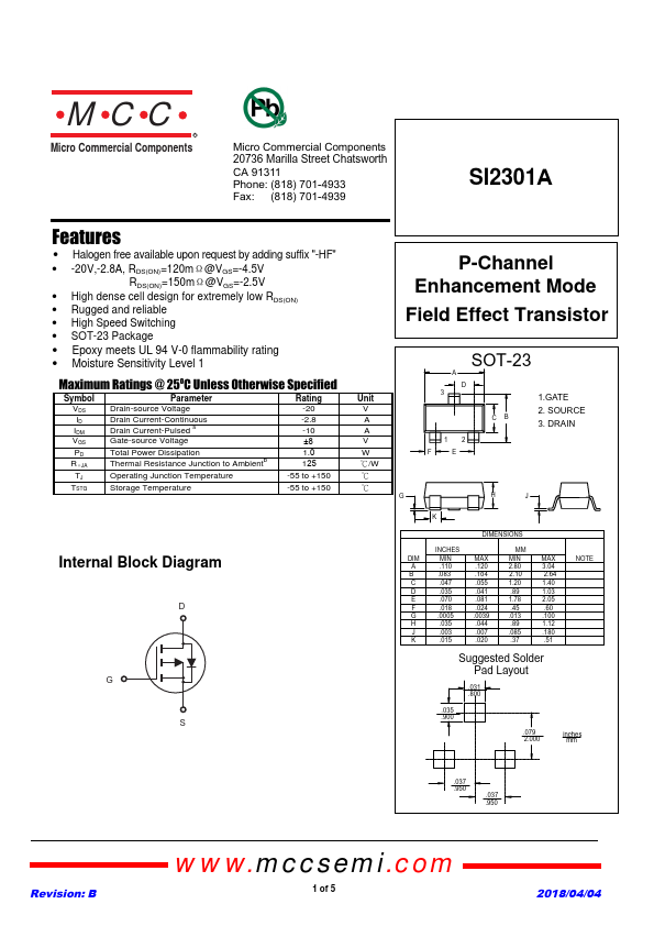
- SOT-23 Package
- Epoxy meets UL 94 V-0 flammability rating
- Moisture Sensitivity Level 1