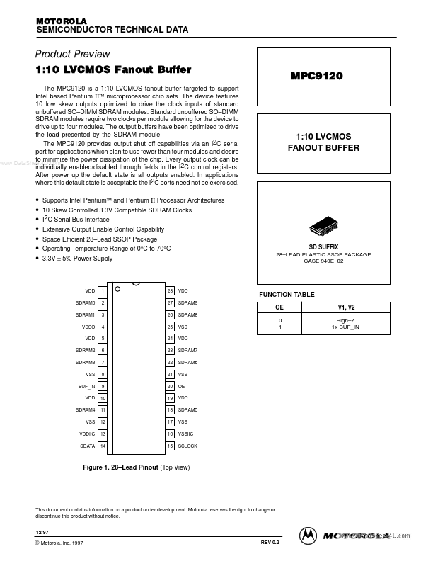
Datasheet4U Logo Datasheet4U.com

MPC9120 - 1:10 LVCMOS FANOUT BUFFER

Datasheet Summary

Description

Pin Name BUF_IN SDRAM0:9 SDATA SCLK OE VDD VSS I/O I O I/O I I

3.3V CMOS clock input 3.3V CMOS SDRAM clock outputs Serial data for configuration control Serial clock input for configuration control.

Features

  • 10 low skew outputs optimized to drive the clock inputs of standard unbuffered SO.
  • DIMM SDRAM modules. Standard unbuffered SO.
  • DIMM SDRAM modules require two clocks per module allowing for the device to drive up to four modules. The output buffers have been optimized to drive the load presented by the SDRAM module. The MPC9120 provides output shut off capabilities via an I2C serial port for.

📥 Download Datasheet

Datasheet preview – MPC9120

Datasheet Details

Part number MPC9120
Manufacturer Motorola
File Size 98.14 KB
Description 1:10 LVCMOS FANOUT BUFFER
Datasheet download datasheet MPC9120 Datasheet
Additional preview pages of the MPC9120 datasheet.
Other Datasheets by Motorola

Full PDF Text Transcription

Click to expand full text
MOTOROLA SEMICONDUCTOR TECHNICAL DATA Product Preview 1:10 LVCMOS Fanout Buffer The MPC9120 is a 1:10 LVCMOS fanout buffer targeted to support Intel based Pentium II™ microprocessor chip sets. The device features 10 low skew outputs optimized to drive the clock inputs of standard unbuffered SO–DIMM SDRAM modules. Standard unbuffered SO–DIMM SDRAM modules require two clocks per module allowing for the device to drive up to four modules. The output buffers have been optimized to drive the load presented by the SDRAM module. The MPC9120 provides output shut off capabilities via an I2C serial port for applications which plan to use fewer than four modules and desire to minimize the power dissipation of the chip. Every output clock can be www.DataSheet4U.
Published: |