MTB16N25E
MOTOROLA
SEMICONDUCTOR TECHNICAL DATA
Order this document by MTB16N25E/D
™ Data Sheet TMOS E-FET.™ High Energy Power FET D2PAK for Surface Mount
Designer's
Motorola Preferred Device
N- Channel Enhancement- Mode Silicon Gate
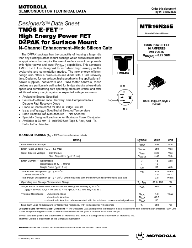
The D2PAK package has the capability of housing a larger die than any existing surface mount package which allows it to be used in applications that require the use of surface mount ponents with higher power and lower RDS(on) capabilities. This advanced TMOS E- FET is designed to withstand high energy in the avalanche and mutation modes. The new energy efficient design also offers a drain- to- source diode with a fast recovery time. Designed for low voltage, high speed switching applications in power supplies, converters and PWM motor controls, these devices are particularly well suited for bridge circuits where diode speed and mutating safe operating areas are critical and offer additional safety margin against unexpected voltage transients.
- Avalanche...