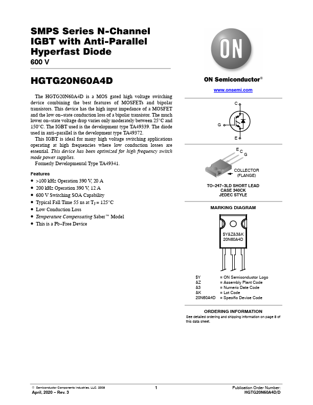
HGTG20N60A4D
ABSOLUTE MAXIMUM RATINGS (TC = 25°C unless otherwise specified)
Parameter
Symbol HGTG20N60A4D Unit
Collector to Emitter Voltage
BVCES
600
V
Collector Current Continuous
At TC = 25°C
At TC = 110°C
IC25
70
A
IC110
40
A
Collector Current Pulsed (Note 1)
Diode Continuous Forward Current
ICM
280
A
IFM110
20
A
Diode Maximum Forward Current
IFM
80
A
Gate to Emitter Voltage Continuous
VGES
±20
V
Gate to Emitter Voltage Pulsed
VGEM
±30
V
Switching Safe Operating Area at TJ = 150°C, (Figure 2)
SSOA
100 A at 600 V
Power Dissipation Total at TC = 25°C
PD
290
W
Power Dissipation Derating TC > 25°C
2.32
W/°C
Operating and Storage Junction Temperature Range
TJ, TSTG
−55 to 150
°C
Maximum Lead Temperature for Soldering
TL
260
°C
Stresses exceeding those listed in the Maximum Ratings table may damage the device. If any of these limits are exceeded, device functionality
should not be assumed, damage may occur and reliability may be affected.
1. Pulse width limited by maximum junction temperature.
ELECTRICAL CHARACTERISTICS (TJ = 25°C unless otherwise specified)
Parameter
Symbol
Test Condition
Min
Collector to Emitter Breakdown Voltage
Collector to Emitter Leakage Current
Collector to Emitter Saturation Voltage
Gate to Emitter Threshold Voltage
Gate to Emitter Leakage Current
Switching SOA
BVCES IC = 250 mA, VGE = 0 V
600
ICES
VCE = 600 V
TJ = 25°C
−
TJ = 125°C
−
VCE(SAT) IC = 20 A, VGE = 15 V
TJ = 25°C
−
TJ = 125°C
−
VGE(TH) IC = 250 mA, VCE = 600 V
4.5
IGES
VGE = ±20 V
−
SSOA TJ = 150°C, RG = 3 W, VGE = 15 V,
100
L = 100 mH, VCE = 600 V
Gate to Emitter Plateau Voltage
On−State Gate Charge
Current Turn−On Delay Time
Current Rise Time
Current Turn−Off Delay Time
Current Fall Time
Turn−On Energy (Note 3)
Turn−Off Energy (Note 2)
Current Turn−On Delay Time
Current Rise Time
Current Turn−Off Delay Time
Current Fall Time
Turn−On Energy (Note 3)
Turn−Off Energy (Note 2)
VGEP
IC = 20 A, VCE = 300 V
−
Qg(ON) IC = 20 A, VCE = 300 V VGE = 15 V
−
VGE = 20 V
−
td(ON)I IGBT and Diode at TJ = 25°C,
−
trI
ICE = 20 A,
VCE = 390 V,
−
td(OFF)I
VGE = 15 V,
RG = 3 W,
−
tfI
L = 500 mH,
−
EON1
Test Circuit Figure 24
−
EON2
−
EOFF
−
td(ON)I IGBT and Diode at TJ = 125°C,
−
trI
ICE = 20 A,
VCE = 390 V,
−
td(OFF)I
VGE = 15 V,
RG = 3 W,
−
tfI
L = 500 mH,
−
EON1
Test Circuit Figure 24
−
EON2
−
EOFF
−
Typ
Max
Unit
−
−
V
−
250
mA
−
2.0
mA
1.8
2.7
V
1.6
2.0
V
5.5
7.0
V
−
±250
nA
−
−
A
8.6
−
V
142
162
nC
182
210
nC
15
−
ns
12
−
ns
73
−
ns
32
−
ns
105
−
mJ
280
350
mJ
150
200
mJ
15
21
ns
13
18
ns
105
135
ns
55
73
ns
115
−
mJ
510
600
mJ
330
500
mJ
www.onsemi.com
2