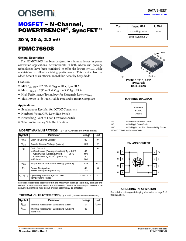
FDMC7660S
FDMC7660S is N-Channel MOSFET manufactured by onsemi.
Description
The FDMC7660S has been designed to minimize losses in power conversion applications. Advancements in both silicon and package technologies have been bined to offer the lowest r DS(on) while maintaining excellent switching performance. This device has the added benefit of an efficient monolithic Schottky body diode.
Features
- Max r DS(on) = 2.2 m W at VGS = 10 V, ID = 20 A
- Max r DS(on) = 2.95 m W at VGS = 4.5 V, ID = 18 A
- High Performance Technology for Extremely Low r DS(on)
- This Device is Pb- Free, Halide Free and is Ro HS pliant
Applications
- Synchronous Rectifier for DC/DC Converters
- Notebook Vcore/GPU Low Side Switch
- Networking Point of Load Low Side Switch
- Tele Secondary Side Rectification
MOSFET MAXIMUM RATINGS (TA = 25°C, unless otherwise noted)
Symbol
Parameter
Ratings Unit
VDS Drain to Source Voltage
VGS Gate to Source Voltage (Note 4)
±20
ID Drain Current
- Continuous (Package Limited) TC = 25°C
- Continuous (Silicon Limited) TC = 25°C
- Continuous TA = 25°C (Note 1a)
- Pulsed
EAS Single Pulse Avalanche Energy (Note 3)
PD Power Dissipation Power Dissipation (Note 1a)
128 m J
TJ, TSTG Operating and Storage Junction Temperature Range
- 55 to +150 °C
Stresses exceeding those listed in the Maximum Ratings table may damage the device. If any of these limits are exceeded, device functionality should not be assumed, damage may occur and reliability may be affected.
THERMAL CHARACTERISTICS (TC = 25°C, unless otherwise...