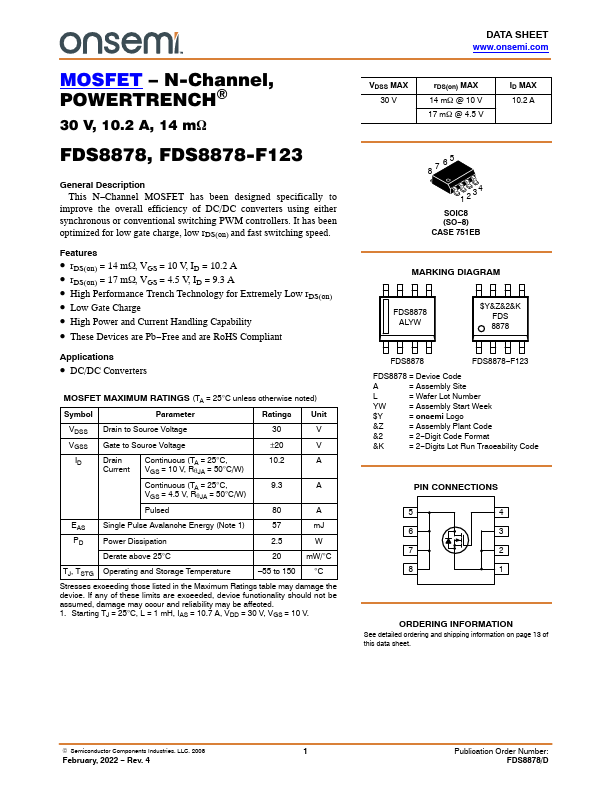
FDS8878
Overview
This N-Channel MOSFET has been designed specifically to improve the overall efficiency of DC/DC converters using either synchronous or conventional switching PWM controllers. It has been optimized for low gate charge, low rDS(on) and fast switching speed.
- rDS(on) = 14 mW, VGS = 10 V, ID = 10.2 A
- rDS(on) = 17 mW, VGS = 4.5 V, ID = 9.3 A
- High Performance Trench Technology for Extremely Low rDS(on)
- Low Gate Charge
- High Power and Current Handling Capability
- These Devices are Pb-Free and are RoHS Compliant