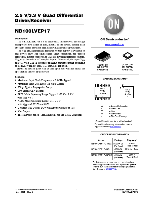
NB100LVEP17 Overview
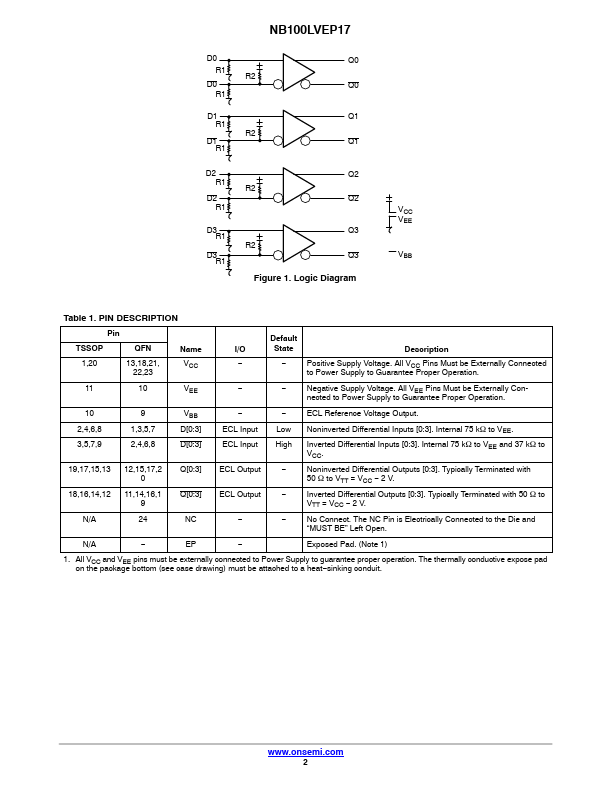
The NB100LVEP17 is a 4-bit differential line receiver. The design incorporates two stages of gain, internal to the device, making it an excellent choice for use in high bandwidth amplifier applications. The VBB pin, an internally generated voltage supply, is available to this device only.
NB100LVEP17 Key Features
- Maximum Input Clock Frequency > 2.5 GHz Typical
- Maximum Input Data Rate > 2.5 Gb/s Typical
- 250 ps Typical Propagation Delay
- Low Profile QFN Package
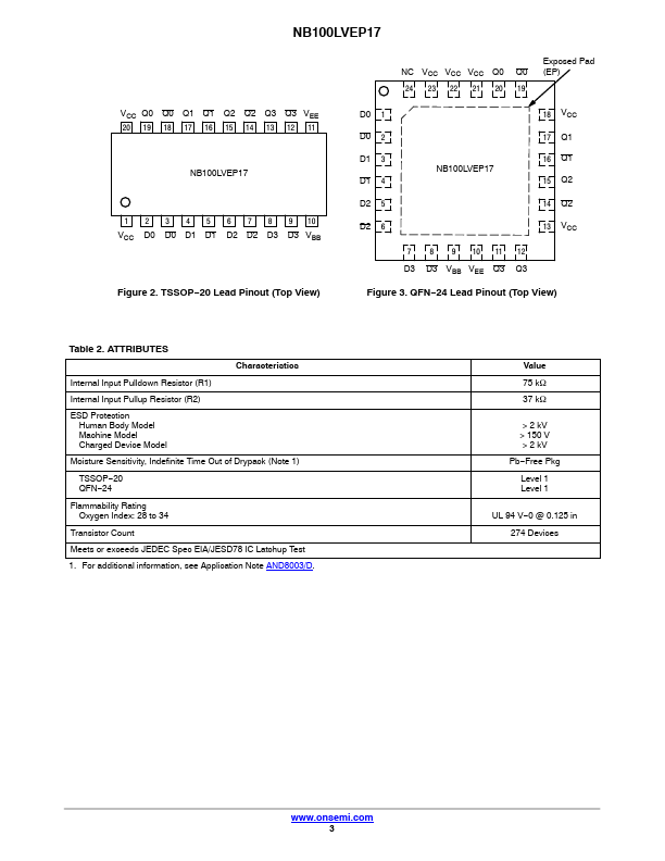
- PECL Mode Operating Range: VCC = 2.375 V to 3.8 V
- NECL Mode Operating Range: VCC = 0 V
- Q Output Will Default LOW with Inputs Open or at VEE
- VBB Output
- These Devices are Pb-Free, Halogen Free and RoHS pliant
- For additional marking information, refer to Application Note AND8002/D