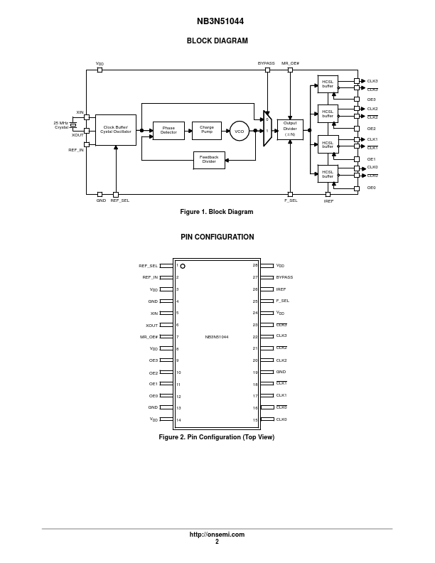
NB3N51044 Description
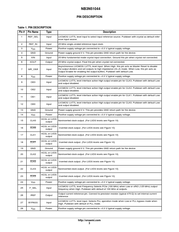
PIN DESCRIPTION Pin # Pin Name Type Description 1 REF_SEL Input LVCMOS/ LVTTL level input to select input reference source.
NB3N51044 Key Features
- Uses 25 MHz Fundamental Crystal or Reference Clock Input
- Four Low Skew HCSL or LVDS Outputs
- Output Frequency Selection of 100 MHz or 125 MHz
- Individual OE Tri-States Outputs
- Master Reset and BYPASS Modes
- PCIe Gen 1, Gen 2, Gen 3 pliant
- Typical Phase Jitter @ 125 MHz (Integrated 1.875 MHz to 20 MHz)
- Typical Cycle-Cycle Jitter @ 100 MHz (10k cycles): 20 ps
- Phase Noise @ 100 MHz
- Operating Supply Voltage Range 3.3 V ±5%