Datasheet4U Logo Datasheet4U.com

NB3N51034 - Quad HCSL - LVDS Clock Generator

Datasheet Summary

Description

Pin Symbol I/O 1 VDDXD Power 2 S0 Input 3 S1 Input 4 S2 Input 5 X1/CLK 6 X2 7 PD Input Output Input 8 OE Input 9 GNDXD 10 IREF 11 CLK3 12 CLK3 13 CLK2 14 CLK2 15 VDDODA 16 GNDODA 17 CLK1 18 CLK1 19 CLK0 20 CLK0 Power Output HCSL or LVDS Output HCSL or LVDS Output HCSL or LVDS Output

Features

  • Uses 25 MHz Fundamental Mode Parallel Resonant Crystal.
  • Power Down Mode.
  • 4 Low Skew HCSL or LVDS Outputs TSSOP.
  • 20 DT SUFFIX CASE 948E NB3N 1034 ALYWG G.
  • OE Tri.
  • States Outputs.
  • Spread of.
  • 0.5%,.
  • 1.0%,.
  • 1.5% and No Spread.
  • PCIe Gen 1, Gen 2, Gen 3, Gen 4 Compliant.
  • Phase Noise (SS OFF) @ 100 MHz: Offset Noise Power A = Assembly Location L = Wafer Lot Y = Year W = Work Week G = Pb.
  • Fre.

📥 Download Datasheet

Datasheet preview – NB3N51034

Datasheet Details

Part number NB3N51034
Manufacturer ON Semiconductor
File Size 434.55 KB
Description Quad HCSL - LVDS Clock Generator
Datasheet download datasheet NB3N51034 Datasheet
Additional preview pages of the NB3N51034 datasheet.
Other Datasheets by ON Semiconductor

Full PDF Text Transcription

Click to expand full text
NB3N51034 3.3V, Crystal to 100MHz/ 200MHz Quad HCSL/LVDS Clock Generator The NB3N51034 is a high precision, low phase noise clock generator that supports spread spectrum designed for PCI Express applications. 
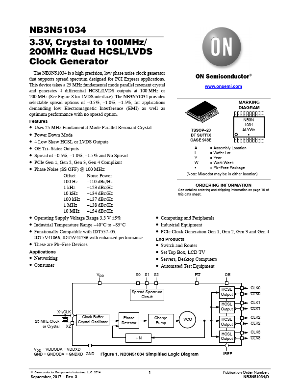
This device takes a 25 MHz fundamental mode parallel resonant crystal and generates 4 differential HCSL/LVDS outputs at 100 MHz or www.onsemi.com 200 MHz (See Figure 8 for LVDS interface). The NB3N51034 provides selectable spread options of −0.5%, −1.0%, −1.5%, for applications demanding low Electromagnetic Interference (EMI) as well as MARKING DIAGRAM optimum performance with no spread option.
Published: |