Datasheet4U Logo Datasheet4U.com

NB3N51044 - Quad HCSL / LVDS Clock Generator

Datasheet Summary

Description

Table 1.

LVCMOS/ LVTTL level input to select input reference source.

Pulldown with crystal as default reference input source.

ended reference input clock.

Features

  • Uses 25 MHz Fundamental Crystal or Reference Clock Input.
  • Four Low Skew HCSL or LVDS Outputs.
  • Output Frequency Selection of 100 MHz or 125 MHz.
  • Individual OE Tri.
  • States Outputs.
  • Master Reset and BYPASS Modes.
  • PCIe Gen 1, Gen 2, Gen 3 Compliant.
  • Typical Phase Jitter @ 125 MHz (Integrated 1.875 MHz to 20 MHz): 0.2 ps.
  • Typical Cycle.
  • Cycle Jitter @ 100 MHz (10k cycles): 20 ps.
  • Phase Noise @ 100 MHz: Off.

📥 Download Datasheet

Datasheet preview – NB3N51044

Datasheet Details

Part number NB3N51044
Manufacturer ON Semiconductor
File Size 130.89 KB
Description Quad HCSL / LVDS Clock Generator
Datasheet download datasheet NB3N51044 Datasheet
Additional preview pages of the NB3N51044 datasheet.
Other Datasheets by ON Semiconductor

Full PDF Text Transcription

Click to expand full text
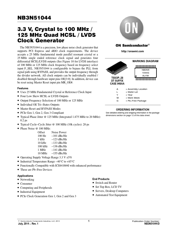
NB3N51044 3.3 V, Crystal to 100 MHz / 125 MHz Quad HCSL / LVDS Clock Generator The NB3N51044 is a precision, low phase noise clock generator that supports PCI Express and sRIO clock requirements. The device accepts a 25 MHz fundamental mode parallel resonant crystal or a 25 MHz single ended reference clock signal and generates four differential HCSL/LVDS outputs (See Figure 10 for LVDS interface) of 100 MHz or 125 MHz clock frequency based on frequency select input F_SEL. NB3N51044 is configurable to bypass the PLL from signal path using BYPASS, and provides the output frequency through the divider network. All clock outputs can be individually enabled / disabled through hardware input pins OE[3:0]. In addition, device can be reset using Master Reset input pin MR_OE#.
Published: |