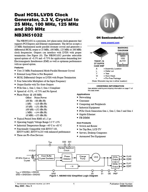
Datasheet4U Logo Datasheet4U.com

NB3N51032 - Dual HCSL/LVDS Clock Generator

Datasheet Summary

Description

Pin Symbol I/O 1 S0 Input 2 S1 Input 3 SS0 Input 4 X1/CLK 5 X2 Input Input 6 OE Input 7 GNDXD Power Supply 8 SS1 Input 9 IREF Output 10 CLK1 HCSL or LVDS Output 11 CLK1 HCSL or LVDS Output 12 VDDODA Power Supply 13 GNDODA Power Supply 14 CLK0 HCSL or LVDS Out

Features

  • Uses 25 MHz Fundamental Mode Parallel Resonant Crystal 1 TSSOP.
  • 16 DT SUFFIX CASE 948F 1032 ALYWG 1 G A = Assembly Location L = Wafer Lot.
  • External Loop Filter is Not Required.
  • HCSL Differential Output or LVDS with Proper Termination.
  • Four Selectable Multipliers of the Input Frequency Y = Year W = Work Week G = Pb.
  • Free Package (Note: Microdot may be in either location).
  • Output Enable with Tri.
  • State Outputs.

📥 Download Datasheet

Datasheet preview – NB3N51032

Datasheet Details

Part number NB3N51032
Manufacturer ON Semiconductor
File Size 435.73 KB
Description Dual HCSL/LVDS Clock Generator
Datasheet download datasheet NB3N51032 Datasheet
Additional preview pages of the NB3N51032 datasheet.
Other Datasheets by ON Semiconductor

Full PDF Text Transcription

Click to expand full text
Dual HCSL/LVDS Clock Generator, 3.3 V, Crystal to 25 MHz, 100 MHz, 125 MHz and 200 MHz NB3N51032 The NB3N51032 is a precision, low phase noise clock generator that supports PCI Express and Ethernet requirements. The device accepts a www.onsemi.com 25 MHz fundamental mode parallel resonant crystal and generates a differential HCSL output at 25 MHz, 100 MHz, 125 MHz or 200 MHz clock frequencies. Outputs can interface with LVDS with proper 16 termination (See Figure 10). The NB3N51032 provides selectable MARKING DIAGRAM 16 NB3N spread options of −0.5% and −0.75% for applications demanding low Electromagnetic Interference (EMI) as well as optimum performance with no spread option.
Published: |