NB3N511
NB3N511 is 3.3V / 5.0V 14MHz to 200MHz PLL Clock Multiplier manufactured by onsemi.
3.3V / 5.0V 14 MHz to 200 MHz PLL Clock Multiplier
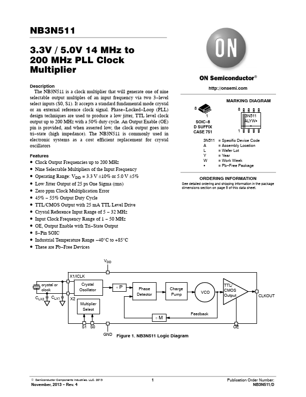
Description The NB3N511 is a clock multiplier that will generate one of nine selectable output multiples of an input frequency via two 3- level select inputs (S0, S1). It accepts a standard fundamental mode crystal or an external reference clock signal. Phase- Locked- Loop (PLL) design techniques are used to produce a low jitter, TTL level clock output up to 200 MHz with a 50% duty cycle. An Output Enable (OE) pin is provided, and when asserted low, the clock output goes into tri- state (high impedance). The NB3N511 is monly used in electronic systems as a cost efficient replacement for crystal oscillators
Features
- Clock Output...