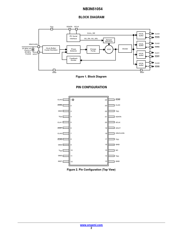
NB3N51054 Description
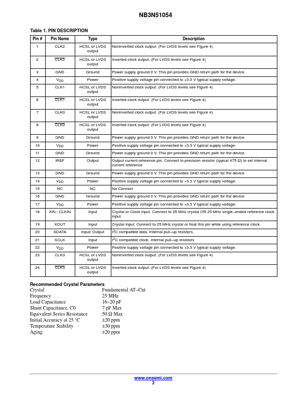
Pin # Pin Name Type 1 CLK2 HCSL or LVDS output Description Noninverted clock output. (For LVDS levels see Figure 4) 2 CLK2 HCSL or LVDS Inverted clock output. (For LVDS levels see Figure 4) outpu.
NB3N51054 Key Features
- Uses 25 MHz Fundamental Crystal or Reference Clock Input
- Four Low Skew HCSL or LVDS Outputs
- I2C Support with Read Back Capability
- Spread of -0.35%, -0.5% and No Spread
- Individual Output Enable/Disable Control through I2C
- PCIe Gen 1, Gen 2, Gen 3 pliant
- Typical Phase Jitter @ 100 MHz (Integrated 12 kHz to 20 MHz)
- Typical Cycle-Cycle Jitter @ 100 MHz (10k cycles): 20 ps
- Phase Noise @ 100 MHz
- Operating Power Supply: 3.3 V ± 5%