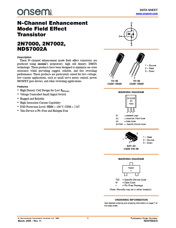
NDS7002A
Overview
- High Density Cell Design for Low RDS(on)
- Voltage Controlled Small Signal Switch
- Rugged and Reliable
- High Saturation Current Capability
- ESD Protection Level: HBM > 100 V, CDM > 2 kV
- This Device is Pb-Free and Halogen Free
| Part Number | Manufacturer | Description |
|---|---|---|
| NDS7002A | National Semiconductor | N-Channel MOSFET |
| NDS7002A | Fairchild Semiconductor | N-Channel MOSFET |
| NDS7000A | National Semiconductor | N-Channel MOSFET |