PLL650-02
PLL650-02 is Low EMI Network LAN Clock manufactured by PhaseLink.
m o .c U 4 t e Features e h
- Full CMOS output swing with 40-mA output drive S output capability. 25-mA drive at TTL level. a t
- Advanced, low power, sub-micron CMOS processes. a
- 25MHz .D fundamental crystal or clock input.
- 4 outputs at 50MHz, 2 outputs selectable at 25MHz or w 125MHz, 1 output selectable at 25MHz or 100MHz. w SDRAM selectable frequencies of 66.6, 75, 83.3, w- 2 100MHz (Double Drive Strength).
- -
- -
- -
Low EMI Network LAN Clock
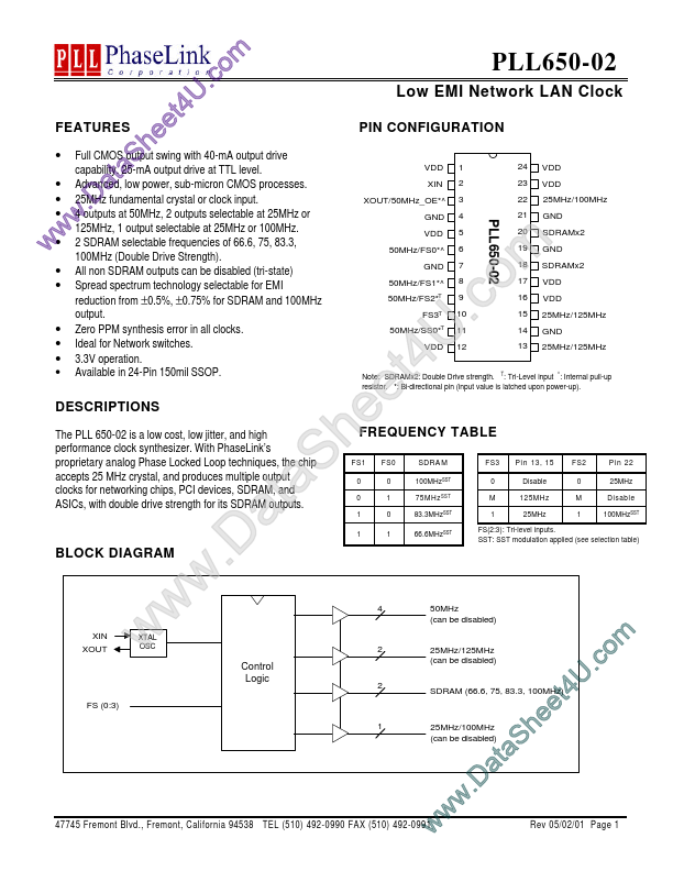
PIN CONFIGURATION
VDD XIN XOUT/50MHz_OE- ^ GND VDD 1 2 3 4 5 6 7 8 9 24 23 22 21 20 19 18 17 16 15 14 13 VDD VDD 25MHz/100MHz GND SDRAMx2 GND
All non SDRAM outputs can be disabled (tri-state) Spread spectrum technology selectable...