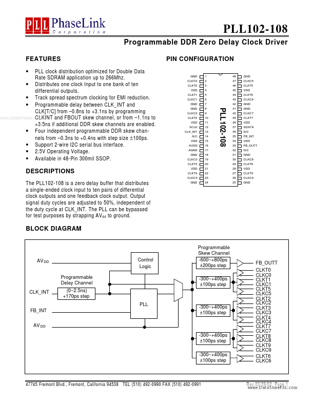
PLL102-108 Description
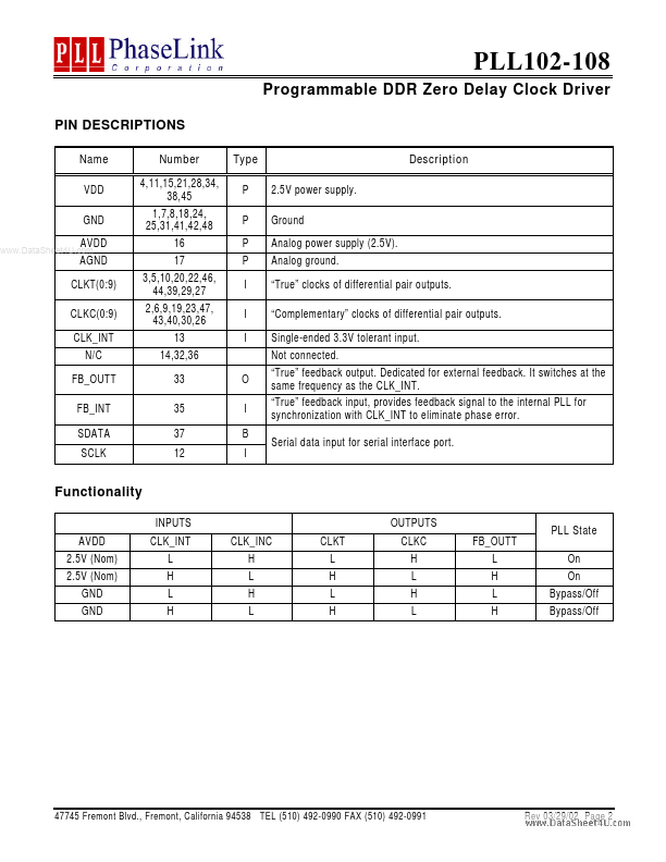
AVDD AGND CLKT(0:9) CLKC(0:9) CLK_INT N/C FB_OUTT FB_INT SDATA SCLK “True” clocks of differential pair outputs. “plementary” clocks of differential pair outputs. Single-ended 3.3V tolerant input.
PLL102-108 Key Features
- Distributes one clock Input to one bank of ten differential outputs
- Track spread spectrum clocking for EMI reduction
- Programmable delay between CLK_INT and CLK[T/C] from -0.8ns to +3.1ns by programming .. CLKINT and FBOUT skew channel, o
- Four independent programmable DDR skew channels from -0.3ns to +0.4ns with step size ± 100ps
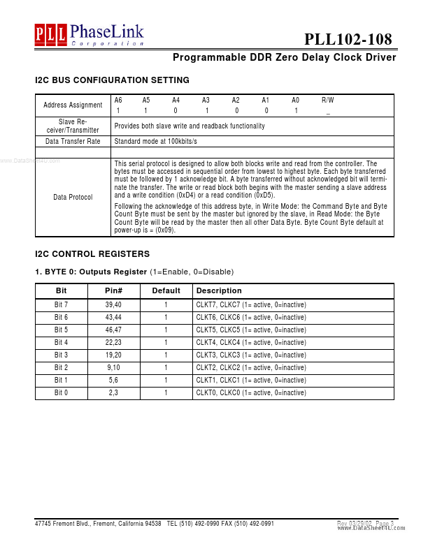
- Support 2-wire I2C serial bus interface
- 2.5V Operating Voltage
- Available in 48-Pin 300mil SSOP