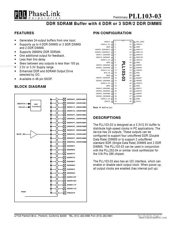
PLL103-03 Description
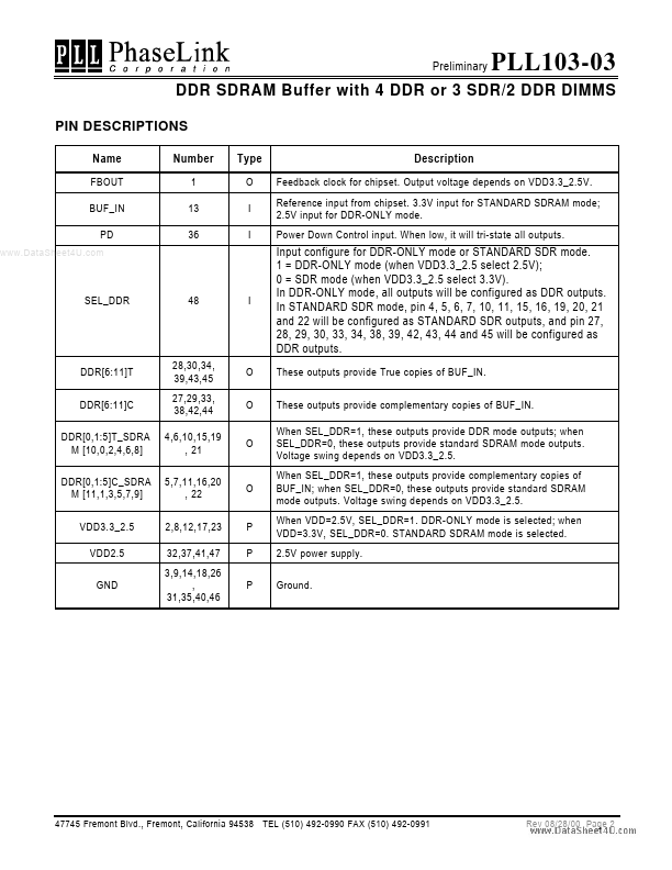
Feedback clock for chipset. Output voltage depends on VDD3.3_2.5V. Reference input from chipset.
PLL103-03 Key Features
- Supports 266MHz DDR SDRAM
- One additional output for feedback
- Less than 5ns delay
- Skew between any outputs is less than 100 ps
- 2.5V or 3.3V Supply range
- Enhanced DDR and SDRAM Output Drive selected by I2C
- Available in 48 pin SSOP