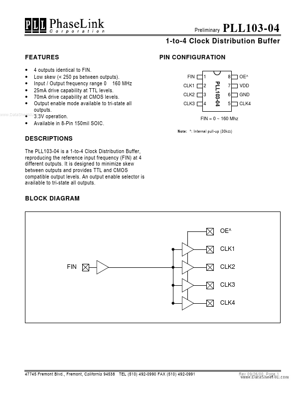
PLL103-04 Description
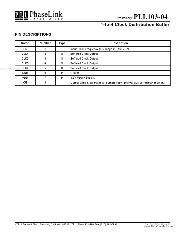
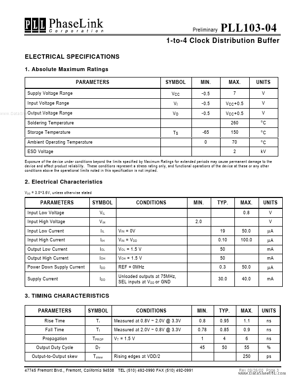
Input Clock Frequency (FIN range 0 ~ 160MHz). Tri-states all outputs if low. Ratings PARAMETERS Supply Voltage Range Input Voltage Range Output Voltage.
PLL103-04 Key Features
- 160 MHz 25mA drive capability at TTL levels. 70mA drive capability at CMOS levels. Output enable mode available to tri-s
- 3.3V operation
- Available in 8-Pin 150mil SOIC