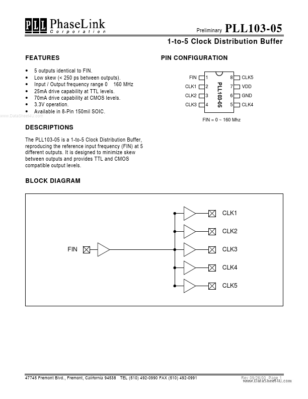
PLL103-05 Description
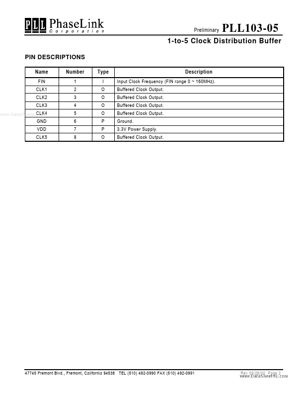
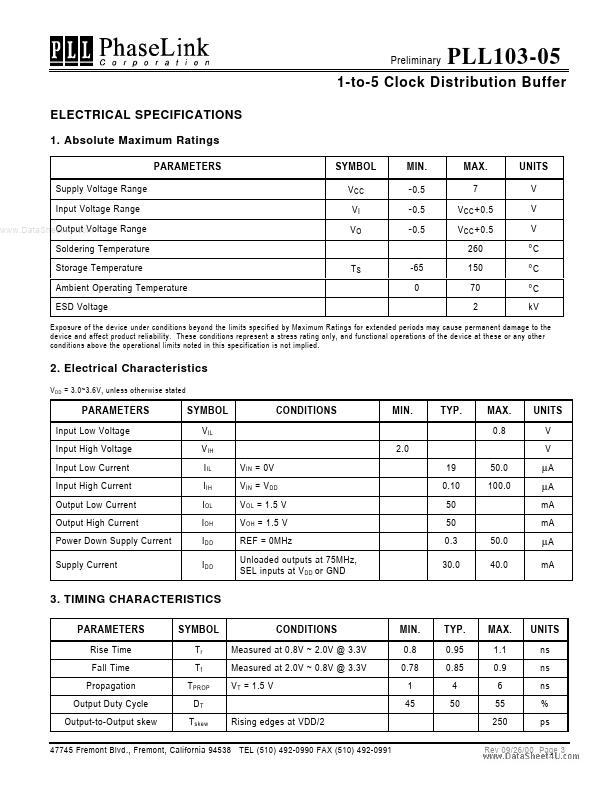
Input Clock Frequency (FIN range 0 ~ 160MHz). Ratings PARAMETERS Supply Voltage Range Input Voltage Range Output Voltage .. Range SYMBOL V CC VI VO MIN.
PLL103-05 Key Features
- 5 outputs identical to FIN. Low skew (< 250 ps between outputs). Input / Output frequency range 0
- 160 MHz 25mA drive capability at TTL levels. 70mA drive capability at CMOS levels. 3.3V operation. Available in 8-Pin 15