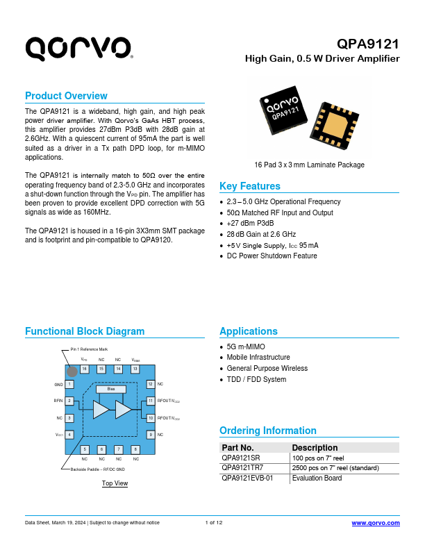
Datasheet4U Logo Datasheet4U.com

QPA9121 - 0.5W Driver Amplifier

Description

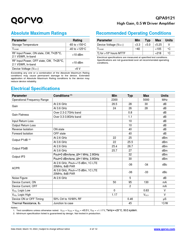
100 pcs on 7” reel 2500 pcs on 7” reel (standard) Evaluation Board Data Sheet, March 19, 2024 | Subject to change without notice 1 of 12 www.qorvo.com QPA9121 ® High Gain, 0.5 W Driver Amplifier Absolute Maximum Ratings Recommended Operating Conditions Parameter Rating Storage Temperature

Features

  • 2.3 .
  •  5.0 GHz Operational Frequency.
  • 50Ω Matched RF Input and Output.
  • +27 dBm P3dB.
  • 28 dB Gain at 2.6 GHz.
  • +5 V Single Supply, ICC 95 mA.
  • DC Power Shutdown Feature Functional Block Diagram Pin 1 Reference Mark VPD NC NC 16 15 14 VBIAS 13 GND 1 RFIN 2 Bias 12 NC 11 RFOUT/VCC2 NC 3 10 RFOUT/VCC2 VCC1 4 9 NC 5 6 7 8 NC NC NC NC Backside Paddle.
  • RF/DC GND Top View.

📥 Download Datasheet

Datasheet Details

Part number QPA9121
Manufacturer Qorvo
File Size 1.10 MB
Description 0.5W Driver Amplifier
Datasheet download datasheet QPA9121 Datasheet

Full PDF Text Transcription (Reference)

The following content is an automatically extracted verbatim text from the original manufacturer datasheet and is provided for reference purposes only.

View original datasheet text
QPA9121 ® High Gain, 0.5 W Driver Amplifier Product Overview The QPA9121 is a wideband, high gain, and high peak power driver amplifier. With Qorvo’s GaAs HBT process, this amplifier provides 27dBm P3dB with 28dB gain at 2.6GHz. With a quiescent current of 95mA the part is well suited as a driver in a Tx path DPD loop, for m-MIMO applications. The QPA9121 is internally match to 50Ω over the entire operating frequency band of 2.3-5.0 GHz and incorporates a shut-down function through the VPD pin. The amplifier has been proven to provide excellent DPD correction with 5G signals as wide as 160MHz. The QPA9121 is housed in a 16-pin 3X3mm SMT package and is footprint and pin-compatible to QPA9120. 16 Pad 3 x 3 mm Laminate Package Key Features • 2.3 – 5.
Published: |