8V19N491-24 Description
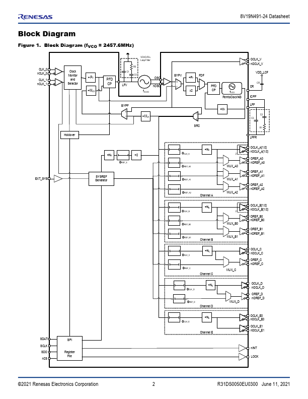
The 8V19N491-24 is a fully integrated FemtoClock NG Jitter Attenuator and Clock Synthesizer that is designed as a high-performance clock solution for conditioning and frequency/phase management of wireless base station radio equipment boards. The device is optimized to deliver excellent phase noise performance as required in GSM, WCDMA, LTE, and LTE-A radio board implementations. The device supports JESD204B...
8V19N491-24 Key Features
- High-performance clock RF-PLL with support for JESD204B/C
- Optimized for low phase noise: -155dBc/Hz (1MHz offset; 245.76MHz clock, and 491.52MHz VCXO)
- Integrated phase noise of 80fs RMS typical (12k-20MHz)
- Dual-PLL architecture
- First PLL stage with external VCXO for clock jitter attenuation
- Second PLL with internal FemtoClockNG PLL: 2457.6MHz
- Four JESD204B channels (device clock and SYSREF
- One clock channel with two outputs
- One VCXO output
- Configurable integer clock frequency dividers