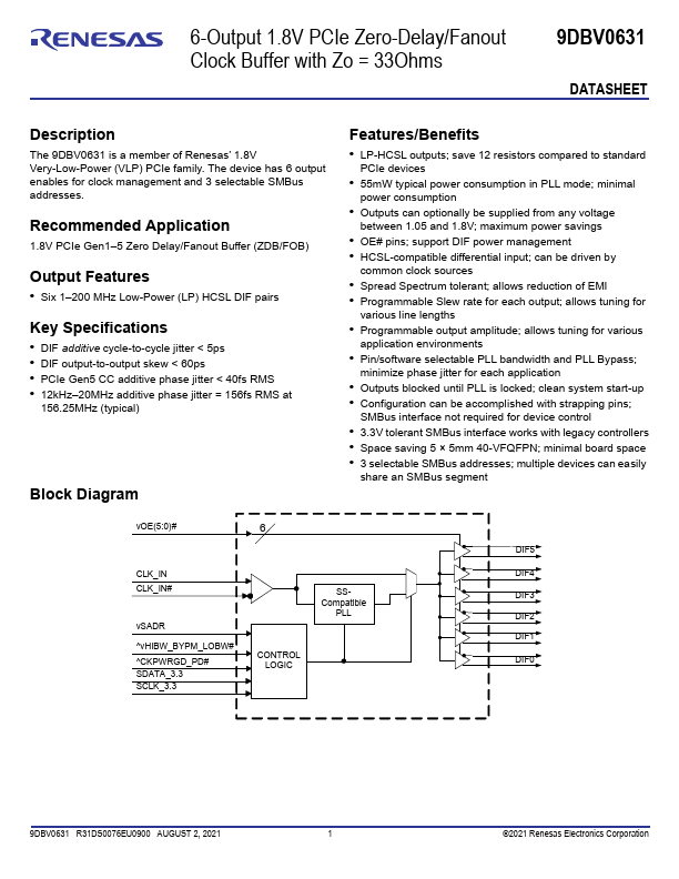
Datasheet4U Logo Datasheet4U.com

9DBV0631 - 6-Output 1.8V PCIe Zero-Delay/Fanout Clock Buffer

General Description

The 9DBV0631 is a member of Renesas’ 1.8V Very-Low-Power (VLP) PCIe family.

The device has 6 output enables for clock management and 3 selectable SMBus addresses.

5 Zero Delay/Fanout Buffer (ZDB/FOB) Output

Key Features

  • Six 1.
  • 200 MHz Low-Power (LP) HCSL DIF pairs Key Specifications.
  • DIF additive cycle-to-cycle jitter < 5ps.
  • DIF output-to-output skew < 60ps.
  • PCIe Gen5 CC additive phase jitter < 40fs RMS.
  • 12kHz.
  • 20MHz additive phase jitter = 156fs RMS at 156.25MHz (typical) Block Diagram Features/Benefits.
  • LP-HCSL outputs; save 12 resistors compared to standard PCIe devices.
  • 55mW typical power consumption in PLL mode; minimal power co.

📥 Download Datasheet

Datasheet Details

Part number 9DBV0631
Manufacturer Renesas
File Size 746.99 KB
Description 6-Output 1.8V PCIe Zero-Delay/Fanout Clock Buffer
Datasheet download datasheet 9DBV0631 Datasheet

Full PDF Text Transcription (Reference)

The following content is an automatically extracted verbatim text from the original manufacturer datasheet and is provided for reference purposes only.

View original datasheet text
6-Output 1.8V PCIe Zero-Delay/Fanout Clock Buffer with Zo = 33Ohms 9DBV0631 DATASHEET Description The 9DBV0631 is a member of Renesas’ 1.8V Very-Low-Power (VLP) PCIe family. The device has 6 output enables for clock management and 3 selectable SMBus addresses. Recommended Application 1.8V PCIe Gen1–5 Zero Delay/Fanout Buffer (ZDB/FOB) Output Features • Six 1–200 MHz Low-Power (LP) HCSL DIF pairs Key Specifications • DIF additive cycle-to-cycle jitter < 5ps • DIF output-to-output skew < 60ps • PCIe Gen5 CC additive phase jitter < 40fs RMS • 12kHz–20MHz additive phase jitter = 156fs RMS at 156.