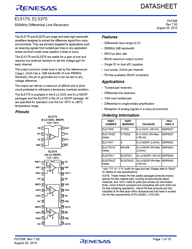
EL5175, EL5375
Absolute Maximum Ratings (TA = +25°C)
Supply Voltage (VS+ to VS-) . . . . . . . . . . . . . . . . . . . . . . . . . . . .12V
Supply Voltage Rate-of-rise (dV/dT) . . . . . . . . . . . . . . . . . . . . 1V/µs
Input Voltage (IN+, IN- to VS+, VS-). . . . . . VS- - 0.3V to VS+ + 0.3V
Differential Input Voltage (IN+ to IN-) . . . . . . . . . . . . . . . . . . . . ±4.8V
Maximum Output Current. . . . . . . . . . . . . . . . . . . . . . . . . . . . ±60mA
Thermal Information
Operating Junction Temperature . . . . . . . . . . . . . . . . . . . . . . +135°C
Ambient Operating Temperature . . . . . . . . . . . . . . . .-40°C to +85°C
Storage Temperature Range . . . . . . . . . . . . . . . . . .-65°C to +150°C
Power Dissipation . . . . . . . . . . . . . . . . . . . . . . . . . . . . . See Curves
Pb-free reflow profile . . . . . . . . . . . . . . . . . . . . . . . . . .see link below
http://www.intersil.com/pbfree/Pb-FreeReflow.asp
CAUTION: Do not operate at or near the maximum ratings listed for extended periods of time. Exposure to such conditions may adversely impact product reliability and
result in failures not covered by warranty.
IMPORTANT NOTE: All parameters having Min/Max specifications are guaranteed. Typ values are for information purposes only. Unless otherwise noted, all tests are
at the specified temperature and are pulsed tests, therefore: TJ = TC = TA
Electrical Specifications VS+ = +5V, VS- = -5V, TA = +25°C, VIN = 0V, RL = 500, RF = 0, RG = OPEN, CL = 2.7pF, Unless Otherwise
Specified.
PARAMETER
DESCRIPTION
CONDITIONS
MIN TYP MAX UNIT
AC PERFORMANCE
BW -3dB Bandwidth
BW
SR
tSTL
tOVR
GBWP
± 0.1dB Bandwidth
Slew Rate
Settling Time to 0.1%
Output Overdrive Recovery Time
Gain Bandwidth Product
AV = 1, CL = 2.7pF
AV = 2, RF = 806, CL = 2.7pF
AV = 10, RF = 806, CL = 2.7pF
AV = 1, CL = 2.7pF
VOUT = 3VP-P, 20% to 80%, RL = 100
VOUT = 3VP-P, 20% to 80%, RL = 500
VOUT = 2VP-P
550
190
20
60
600
900
10
20
200
MHz
MHz
MHz
MHz
V/µs
V/µs
ns
ns
MHz
VREFBW (-3dB) VREF -3dB Bandwidth
VREFSR
VREF Slew Rate
VN Input Voltage Noise
IN Input Current Noise
HD2
Second Harmonic Distortion
HD2
Second Harmonic Distortion
HD3
Third Harmonic Distortion
HD3
Third Harmonic Distortion
dG Differential Gain at 3.58MHz
d Differential Phase at 3.58MHz
eS Channel Separation (EL5375)
INPUT CHARACTERISTICS
AV = 1, CL = 2.7pF
VOUT = 2VP-P, 20% to 80%
At f = 10kHz
At f = 10kHz
VOUT = 1VP-P, 5MHz
VOUT = 1VP-P, 5MHz
VOUT = 1VP-P, 5MHz
VOUT = 1VP-P, 5MHz
RL = 150AV = 2
RL = 150AV = 2
At f = 100kHz
450
1000
21
2.7
-70
-66
-94
-84
0.1
0.1
90
MHz
V/µs
nV/Hz
pA/Hz
dBc
dBc
dBc
dBc
%
°
dB
VOS
Input Referred Offset Voltage
EL5175
EL5375
-3 ±40 mV
-3 ±30 mV
IIN
RIN
CIN
DMIR
Input Bias Current (VIN, VINB, VREF)
Differential Input Resistance
Differential Input Capacitance
Differential Mode Input Range
-25 -12.5
-6
150
1
±2.1 ±2.3 ±2.5
µA
k
pF
V
CMIR
Common Mode Input Range at VIN+, VIN-
-4.3
+3.3
V
FN7306 Rev 7.00
August 25, 2010
Page 2 of 15