Datasheet4U Logo Datasheet4U.com

IDTCV123 - PROGRAMMABLE CLOCK

Description

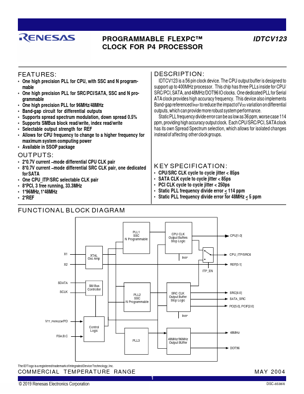
IDTCV123 is a 56 pin clock device.

The CPU output buffer is designed to support up to 400MHz processor.

This chip has three PLLs inside for CPU/ SRC/PCI, SATA, and 48MHz/DOT96 IO clocks.

Features

  • One high precision PLL for CPU, with SSC and N programmable.
  • One high precision PLL for SRC/PCI/SATA, SSC and N programmable.
  • One high precision PLL for 96MHz/48MHz.
  • Band-gap circuit for differential outputs.
  • Supports spread spectrum modulation, down spread 0.5%.
  • Supports SMBus block read/write, index read/write.
  • Selectable output strength for REF.
  • Allows for CPU frequency to change to a higher frequency for maximum system.

📥 Download Datasheet

Datasheet Details

Part number IDTCV123
Manufacturer Renesas
File Size 252.00 KB
Description PROGRAMMABLE CLOCK
Datasheet download datasheet IDTCV123 Datasheet
Other Datasheets by Renesas

Full PDF Text Transcription

Click to expand full text
IDTCV123 PROGRAMMABLE FLEXPC™ CLOCK FOR P4 PROCESSOR COMMERCIAL TEMPERATURE RANGE PROGRAMMABLE FLEXPC™ CLOCK FOR P4 PROCESSOR IDTCV123 FEATURES: • One high precision PLL for CPU, with SSC and N programmable • One high precision PLL for SRC/PCI/SATA, SSC and N programmable • One high precision PLL for 96MHz/48MHz • Band-gap circuit for differential outputs • Supports spread spectrum modulation, down spread 0.5% • Supports SMBus block read/write, index read/write • Selectable output strength for REF • Allows for CPU frequency to change to a higher frequency for maximum system computing power • Available in SSOP package OUTPUTS: • 2*0.7V current –mode differential CPU CLK pair • 8*0.
Published: |