Description
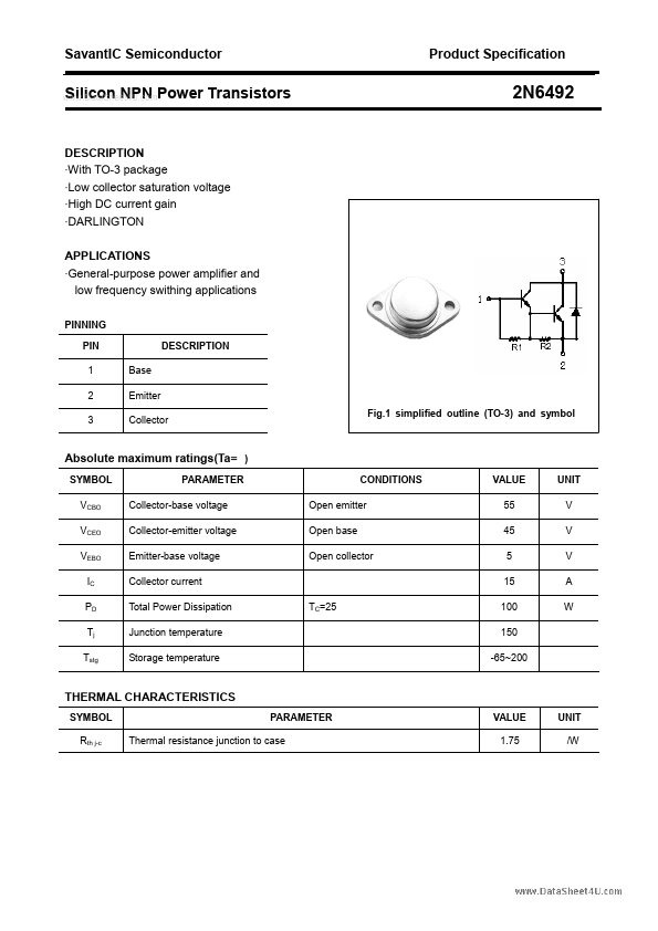
With TO-3 package - Low collector saturation voltage - High DC current gain - DARLINGTON APPLICATIONS - General-purpose power amplifier and low frequency swithing applications PINNING PIN 1 2 3 Base Emitter Collector Fig.1 simplified outline (TO-3) and symbol DESCRIPTION SYMBOL VCBO VCEO VEBO IC PD Tj Tstg PARAMETER Collector-base voltage Collector-emitter voltage Emitter-base voltage Collector current Total Power Dissipation Junction temperature Storage temperature TC=25 CONDITIONS Open emitter Open base Open collector VALUE 55 45 5 15 100 150 -65~200 UNIT V V V A W SYMBOL Rth j-c PARAMETER SavantIC Semiconductor Product Specification Silicon NPN Power Transistors 2N6492 CHARACTERISTICS Tm=25 unless otherwise specified PARAMETER CONDITIONS MIN TYP. MAX UNIT SYMBOL VCEO(SUS) VCEsat VBEsat VBE ICEO ICEX IEBO hFE-1 hFE-2 Collector-emitter sustaining voltage IC=0.1 A ;IB=0 IC=10A ;IB=100mA IC=10A ;IB=100mA IC=3A ; VCE=4V VCE=40V; IB=0 VCE=55V; VBE(off)=-1.5V VEB=5V; IC=0 IC=3A ; VCE=4V IC=15A ; VCE=4V 45 V Collector-emitter saturation voltage 3.0 V Base-emitter saturation voltage 4.0 V Base-emitter on voltage 2.8 V Collector cut-off current 1.0 mA Collector cut-off current 0.5 mA Emitter cut-off current 3.0 mA DC current gain 500 DC current gain 100 2 SavantIC Semiconductor Product Specification Silicon NPN Power Transistors PACKAGE OUTLINE 2N6492 Fig.2 outline dimensions (unindicated tolerance:±0.10mm) 3.