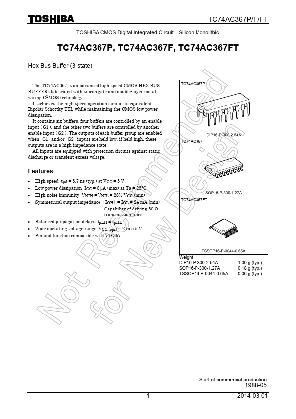
TC74AC367FN Overview
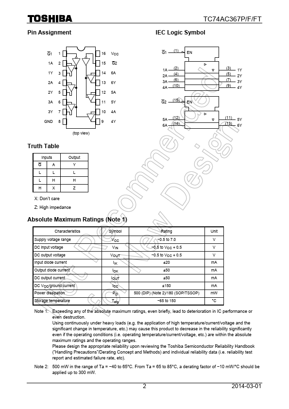
It achieves the high speed operation similar to equivalent Bipolar Schottky TTL while maintaining the CMOS low power dissipation. four buffers are controlled by an enable input ( G1 ), and the other two buffers are controlled by another enable input ( G2 ). The outputs of each buffer group are enabled when G1 and/or G2 inputs are held low;.
TC74AC367FN Key Features
- High speed: tpd = 3.7 ns (typ.) at VCC = 5 V
- Low power dissipation: ICC = 8 µA (max) at Ta = 25°C
- High noise immunity: VNIH = VNIL = 28% VCC (min)
- Symmetrical output impedance: |IOH| = IOL = 24 mA (min)
- Balanced propagation delays: tpLH ∼- tpHL
- Wide operating voltage range: VCC (opr) = 2 to 5.5 V
- Pin and function patible with 74F367