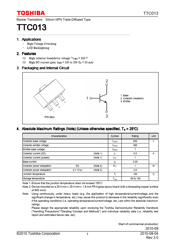
Bipolar Transistors Silicon NPN Triple-Diffused Type
TTC013
1. Applications
• High-Voltage Switching
• LCD Backlighting
2. Features
(1) High collector breakdown voltage: VCEO = 350 V
(2) High DC current gain: hFE = 100 to 200 (IC = 50 mA)
3. Packaging and Internal Circuit
TTC013
1. Base
2. Collector (Heatsink)
3. Emitter
PW-Mini
4. Absolute Maximum Ratings (Note) (Unless otherwise specified, Ta = 25)
Characteristics
Symbol
Rating
Unit
Collector-base voltage
.
VCBO
600
V
Collector-emitter voltage
Emitter-base voltage
VCEO
350
VEBO
7
Collector current (DC)
(Note 1)
IC
0.5
A
Collector current (pulsed)
Base current
(Note 1)
ICP
IB
1
0.25
Collector power dissipation
DC
(Note 2)
PC
1
W
Collector power dissipation
(t = 10 s)
(Note 2)
2.5
Junction temperature
Tj
150
Storage temperature
Tstg
-55 to 150
Note 1: Ensure that the junction temperature does not exceed 150.
Note 2: Device mounted on a 25.4 mm x 25.4 mm x 1.6 mm FR-4 glass epoxy board (with a dissipating copper surface
of 645 mm2)
Note: Using continuously under heavy loads (e.g. the application of high temperature/current/voltage and the
significant change in temperature, etc.) may cause this product to decrease in the reliability significantly even
if the operating conditions (i.e. operating temperature/current/voltage, etc.) are within the absolute maximum
ratings.
Please design the appropriate reliability upon reviewing the Toshiba Semiconductor Reliability Handbook
("Handling Precautions"/"Derating Concept and Methods") and individual reliability data (i.e. reliability test
report and estimated failure rate, etc).
©2015 Toshiba Corporation
1
Start of commercial production
2010-09
2015-08-04
Rev.3.0