Part number:
TW015Z120C
Manufacturer:
File Size:
643.06 KB
Description:
Silicon carbide n-channel mosfet.
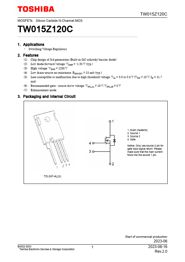
TW015Z120C Features
* (1) Chip design of 3rd generation (Built-in SiC schottky barrier diode) (2) Low diode forward voltage: VDSF = -1.35 V (typ.) (3) High voltage: VDSS = 1200 V (4) Low drain-source on-resistance: RDS(ON) = 15 mΩ (typ.) (5) Less susceptible to malfunction due to high threshold voltage: Vth = 3.0 to 5.0
TW015Z120C Datasheet (643.06 KB)
Datasheet Details
TW015Z120C
643.06 KB
Silicon carbide n-channel mosfet.
📁 Related Datasheet
TW015Z65C Silicon Carbide N-Channel MOSFET (Toshiba)
TW015N120C Silicon N-channel MOSFET (Toshiba)
TW015N65C Silicon Carbide N-Channel MOSFET (Toshiba)
TW027N65C Silicon N-channel MOSFET (Toshiba)
TW045N120C Silicon N-channel MOSFET (Toshiba)
TW048N65C Silicon N-channel MOSFET (Toshiba)
TW050LH9CTLCM Display Module (TOPWIN)
TW-0x-xx-F-D-xxx-SM (TW Series) SMT BOARD STACKERS (Samtec)
TW015Z120C Distributor