UF3C065030T3S
UF3C065030T3S is MOSFET manufactured by UnitedSiC.
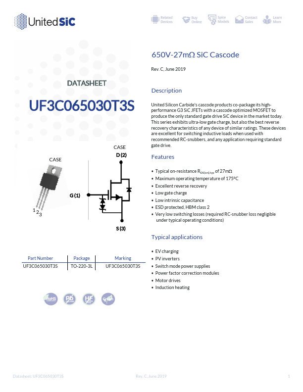
Description
United Silicon Carbide's cascode products co-package its highperformance G3 Si C JFETs with a cascode optimized MOSFET to produce the only standard gate drive Si C device in the market today. This series exhibits ultra-low gate charge, but also the best reverse recovery characteristics of any device of similar ratings. These devices are excellent for switching inductive loads when used with remended RC-snubbers, and any application requiring standard gate drive.
Features w Typical on-resistance RDS(on),typ of 27m W w Maximum operating temperature of 175°C w Excellent reverse recovery w Low gate charge w Low intrinsic capacitance w ESD protected, HBM class 2 w Very low switching losses (required RC-snubber loss negligible . under typical operating conditions)
Typical applications w EV charging w PV inverters w Switch mode power supplies w Power factor correction modules w Motor drives w Induction heating
Datasheet: UF3C065030T3S
Rev. C, June 2019
Maximum Ratings
Parameter Drain-source voltage Gate-source voltage
Continuous drain current 1
Pulsed drain current 2 Single pulsed avalanche energy 3 Power dissipation Maximum junction temperature Operating and storage temperature Max. lead temperature for soldering, 1/8” from case for 5 seconds
1. Limited by TJ,max 2. Pulse width tp limited by TJ,max 3. Starting TJ = 25°C
Symbol VDS VGS
IDM EAS Ptot TJ,max TJ, TSTG
Test Conditions
DC TC = 25°C TC = 100°C TC = 25°C L=15m H, IAS =4A TC = 25°C
Value 650 -25 to +25 85 62 230 120 441 175 -55 to 175
Units V V A A A m J W °C °C
°C
Thermal Characteristics
Parameter Thermal resistance, junction-to-case
Symbol Rq JC
Test Conditions
Min
Value Typ
Max
Units
0.26 0.34 °C/W
Datasheet: UF3C065030T3S
Rev. C, June 2019
Electrical Characteristics (TJ = +25°C unless otherwise specified) Typical Performance
- Static
Parameter Drain-source breakdown voltage Total drain leakage current
Total gate leakage current
Drain-source on-resistance Gate threshold...