SiR404DP
SiR404DP is N-Channel MOSFET manufactured by Vishay.
FEATURES
- Halogen-free According to IEC 61249-2-21 Definition
- Trench FET® Gen III Power MOSFET
- 100 % Rg Tested
- 100 % UIS Tested
- 2.5 V and 3.3 V Gate Drive MOSFET for dc-to-dc Applications
- pliant to Ro HS Directive 2002/95/EC
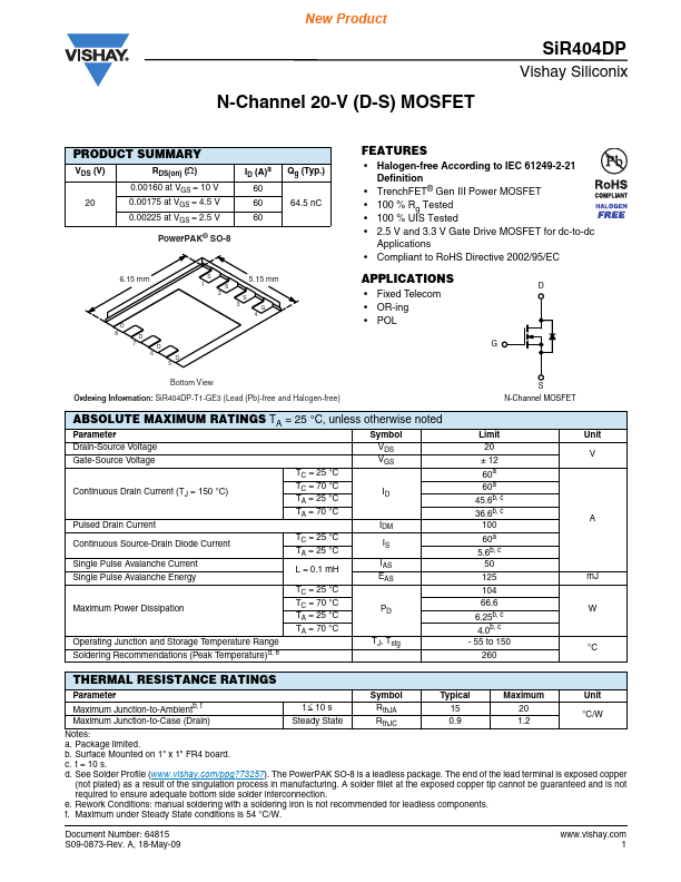
Power PAK® SO-8
6.15 mm
S 1 2 3 S S
5.15 mm
APPLICATIONS
- Fixed Tele
- OR-ing
- POL
G 4
D 8 7 6 5 D D D
Bottom View Ordering Information: Si R404DP-T1-GE3 (Lead (Pb)-free and Halogen-free)
S N-Channel MOSFET
ABSOLUTE MAXIMUM RATINGS TA = 25 °C, unless otherwise noted
Parameter Drain-Source Voltage Gate-Source Voltage TC = 25 °C TC = 70 °C TA = 25 °C TA = 70 °C TC = 25 °C TA = 25 °C L = 0.1 m H TC = 25 °C TC = 70 °C TA = 25 °C TA = 70 °C Symbol VDS VGS ID Limit 20 ± 12 60a 60a 45.6b, c 36.6b, c 100 60a 5.6b, c 50 125 104 66.6 6.25b, c 4.0b, c
- 55 to 150 260 Unit V
Continuous Drain Current (TJ = 150 °C)
Pulsed Drain Current Continuous Source-Drain Diode Current Single Pulse Avalanche Current Single Pulse Avalanche Energy
IDM IS IAS EAS PD
A m J
Maximum Power Dissipation
Operating Junction and Storage Temperature Range Soldering Remendations (Peak Temperature)d, e
TJ, Tstg
°C
THERMAL RESISTANCE RATINGS
Parameter b, f
Maximum Junction-to-Ambient °C/W Rth JC Maximum Junction-to-Case (Drain) Notes: a. Package limited. b. Surface Mounted on 1" x 1" FR4 board. c. t = 10 s. d. See Solder Profile (.vishay./ppg?73257). The Power PAK SO-8 is a leadless package. The end of the lead terminal is exposed copper (not plated) as a result of the singulation process in manufacturing. A solder fillet at the exposed copper tip cannot be guaranteed and is not required to ensure adequate bottom side solder interconnection. e. Rework Conditions: manual soldering with a soldering iron is not remended for leadless ponents. f. Maximum under Steady State conditions is 54 °C/W. Document Number: 64815 S09-0873-Rev. A, 18-May-09 .vishay. 1 t ≤ 10 s Steady State
Symbol Rth JA
Typical 15 0.9
Maximum 20...