Datasheet Details
| Part number | ADCLK854 |
|---|---|
| Manufacturer | Analog Devices |
| File Size | 724.65 KB |
| Description | Low Power Clock Fanout Buffer |
| Datasheet |
 ADCLK854 Datasheet ADCLK854 Datasheet
|

|
|
| Part number | ADCLK854 |
|---|---|
| Manufacturer | Analog Devices |
| File Size | 724.65 KB |
| Description | Low Power Clock Fanout Buffer |
| Datasheet |
ADCLK854 Datasheet
|
|
|
|
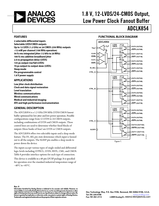
The ADCLK854 is a 1.2 GHz/250 MHz LVDS/CMOS fanout buffer optimized for low jitter and low power operation.
📁 Similar Datasheet