Datasheet Details
- Part number
- CY24271
- Manufacturer
- Cypress Semiconductor
- File Size
- 699.91 KB
- Datasheet
-
 CY24271-CypressSemiconductor.pdf
- Description
- Clock Generator
 CY24271-CypressSemiconductor.pdf
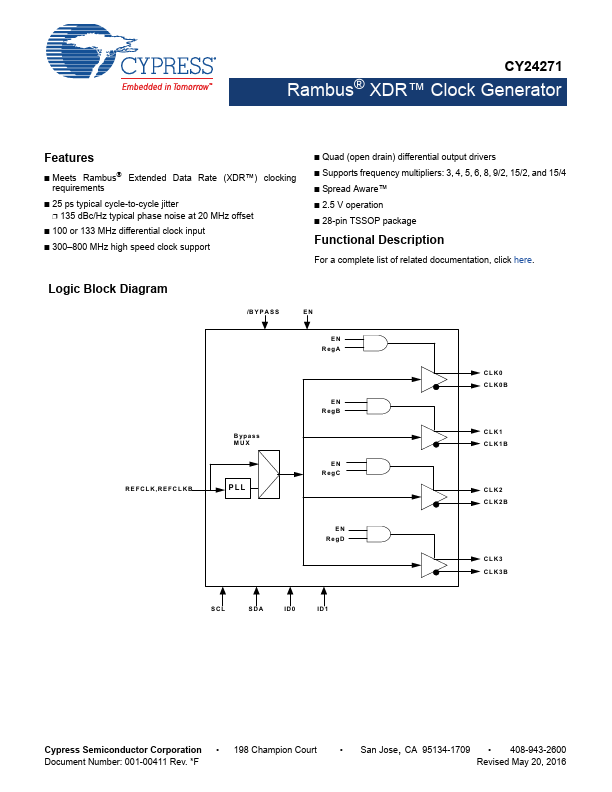
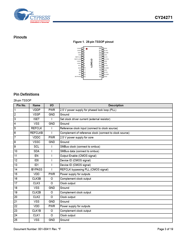
For a complete list of related documentation, click here. 198 Champion Court Document Number: 001-00411 Rev. F San Jose, CA 95134-1709 408-943-2600 Revised May 20, 2016 CY24271 Contents Pinouts
📁 CY24271 Similar Datasheet