Description
Functional Description
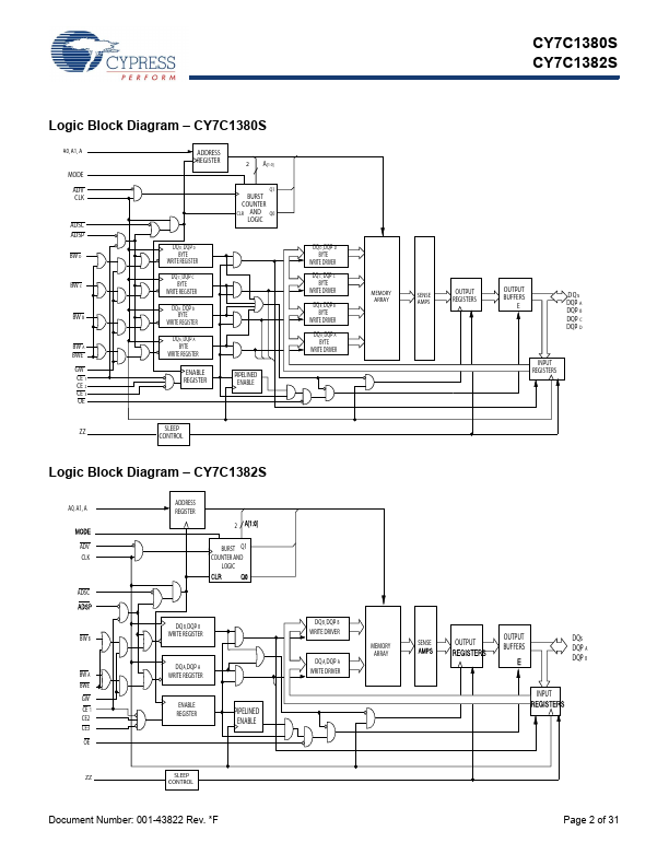
The CY7C1380S/CY7C1382S SRAM integrates 524,288 × 36 and 1,048,576 × 18 SRAM cells with advanced synchronous peripheral circuitry and a two-bit counter for internal burst operation.All synchronous inputs are gated by registers controlled by a positive edge triggered clock input (CLK).The synchronous inputs include all addresses, all data inputs, address-pipelining chip enable (CE1), depth-expansion chip enables (CE2 and CE3), burst control inputs (ADSC, ADSP, and ADV),
Features
- Supports bus operation up to 167 MHz.
- Available speed grade is 167 MHz.
- Registered inputs and outputs for pipelined operation.
- 3.3 V core power supply.
- 2.5 V or 3.3 V I/O power supply.
- Fast clock-to-output times.
- 3.4 ns (for 167 MHz device).
- Provides high-performance 3-1-1-1 access rate.
- User selectable burst counter supporting Intel Pentium®
interleaved or linear burst sequences.
- Separate processor and controller address strobes.
- Synchro.
 CY7C1380S-Cypress.pdf