Datasheet Details
| Part number | M53D256328A |
|---|---|
| Manufacturer | ESMT |
| File Size | 2.26 MB |
| Description | LPDDR SDRAM |
| Datasheet |
 M53D256328A-ESMT.pdf M53D256328A-ESMT.pdf
|
| Part number | M53D256328A |
|---|---|
| Manufacturer | ESMT |
| File Size | 2.26 MB |
| Description | LPDDR SDRAM |
| Datasheet |
M53D256328A-ESMT.pdf
|
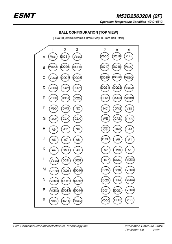
Ball Name Function A0~A11, BA0~BA1 Address inputs - Row address A0~A11 - Column address A0~A8 A10/AP : AUTO Precharge BA0~BA1: Bank selects (4 Banks) DQ0~DQ31 Data-in/Data-out RAS CAS WE VSS VDD DQS0~DQS3 Row address strobe Column address strobe Write enable Ground Power Bi-directional Data Strobe.DQS0 corresponds to the data on DQ0~DQ7; DQS1 correspond to the data on DQ8~DQ15; DQS2 correspond to the data on DQ16~DQ23; DQS3 correspond to the data on DQ24~DQ31. Ball Name DM0~DM3 CLK, CLK
📁 M53D256328A Similar Datasheet